
Digital Signal Processor Product Preview

www.ti.com
PRODUCT PREVIEW
TMS320C6454
Fixed-Point Digital Signal Processor
SPRS311A – APRIL 2006 – REVISED DECEMBER 2006
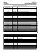
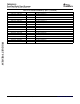
C6454 Revision History (continued)
SEE ADDITIONS/MODIFICATIONS/DELETIONS
Section 3.4.2 Peripheral Configuration Register 0 Description:
Updated paragraph and added Note
Changed all bit field resets to R/W-0 and updated Figure 3-4 , Peripheral Configuration Register 0
(PERCFG0)
Updated Table 3-7 , Peripheral Configuration Register 0 (PERCFG0) Field Descriptions
Section 3.4.5 EMAC Configuration Register (EMACCFG) Description:
Changed bits 23:19 reset value to R/W- 0001b and moved in RMII_RST field to bit 18 Figure 3-8 , EMAC
Configuration Register (EMACCFG)
Updated Reserved Bits 31:19 Description and RMII_RST Bit 18 Description Values 0 and 1 in Table 3-11 ,
EMAC Configuration Register (EMACCFG) Field Descriptions
Section 3.7 Deleted Debugging Considerations
Added new section, Pullup/Pulldown Resistors
Section 3.8 Configuration Examples:
Added comments for AEA[12], AEA[11], and AEA[3] and changed SYSCLK3 to SYSCLK 4 in comment for
AEA[4] in Figure 3-12 , Configuration Example A, and Figure 3-13 , Configuration Example B
Section 5.1 Memory Architecture:
Updated paragraphs
Updated Figure 5-4 , TMS320C6454 L2 Memory Configurations
Section 6 Device Operating Conditions:
Updated Section 6.1 , Absolute Maximum Ratings Over Operating Case Temperature Range
Updated Section 6.2 , Recommended Operating Conditions
Updated Section 6.3 , Electrical Characteristics Over Recommended Ranges of Supply Voltage and
Operating Case Temperature
Section 7.3.1 Power-Supply Sequencing:
Updated paragraph
Deleted Power-Supply Sequence (Option 1) figure and Timing Requirements for Power-Supply Sequence
(Option 1) table
Section 7.3.4 Preserving Boundary-Scan Functionality on RGMII and DDR2 Memory Pins section:
Added DV
DD15MON
to paragraph and list
Section 7.4 Enhanced Direct Memory Access (EDMA3) Controller:
Changed "4 Quick DMA (QDMA) channels" to " 8 Quick DMA (QDMA) channels"
Section 7.4.1 EDMA3 Device-Specific Information:
Updated paragraph
Section 7.4.3 EDMA3 Peripheral Register Description(s):
Changed Table 7-4 title to EDMA3 Channel Controller Registers
Updated Hex Address Ranges for Parameter Sets 7, 9, 254, and 255 on Table 7-5 , EDMA3 Parameter RAM
Added Table 7-6 , EDMA3 Transfer Controller 0 Registers, Table 7-7 , EDMA3 Transfer Controller 1
Registers, Table 7-8 , EDMA3 Transfer Controller 2 Registers, and Table 7-9 , EDMA3 Transfer Controller 3
Registers
Section 7.5.1 Interrupt Sources and Interrupt Controller:
Changed Event Number 80 to Reserved in Table 7-10 , C6454 DSP Interrupts
Section 7.6 Reset Controller:
Updated System Reset Effect(s), and added Footnote (2) in Table 7-12 , Reset Types
Deleted System Reset Timing figure
Section 7.6.7 Reset Electrical Data/Timing:
Updated Note
Added new Footnote (3) and renumbered Footnotes to (4) and (5) in Table 7-14 , Timing Requirements for
Reset
Section 7.7 PLL1 and PLL1 Controller:
Updated Figure 7-10 , PLL1 and PLL1 Controller
Section 7.7.1 PLL1 Controller Device-Specific Information:
Updated SYSCLK4 bullet
Updated paragraphs
Updated Footnote (1) in Table 7-16 , PLL1 Clock Frequency Ranges
Submit Documentation Feedback Revision History 219