
Digital Signal Processor Product Preview


www.ti.com
PRODUCT PREVIEW
7.16.2 PCI Peripheral Register Description(s)
TMS320C6454
Fixed-Point Digital Signal Processor
SPRS311A – APRIL 2006 – REVISED DECEMBER 2006
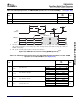
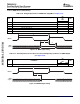
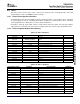
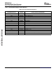
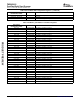
Table 7-97. PCI Configuration Registers
PCI HOST ACCESS
ACRONYM PCI HOST ACCESS REGISTER NAME
HEX ADDRESS OFFSET
0x00 PCIVENDEV Vendor ID/Device ID
0x04 PCICSR Command/Status
0x08 PCICLREV Class Code/Revision ID
0x0C PCICLINE BIST/Header Type/Latency Timer/Cacheline Size
0x10 PCIBAR0 Base Address 0
0x14 PCIBAR1 Base Address 1
0x18 PCIBAR2 Base Address 2
0x1C PCIBAR3 Base Address 3
0x20 PCIBAR4 Base Address 4
0x24 PCIBAR5 Base Address 5
0x28 - 0x2B - Reserved
0x2C PCISUBID Subsystem Vendor ID/Subsystem ID
0x30 - Reserved
0x34 PCICPBPTR Capabilities Pointer
0x38 - 0x3B - Reserved
0x3C PCILGINT Max Latency/Min Grant/Interrupt Pin/Interrupt Line
0x40 - 0x7F - Reserved
C64x+ Peripheral Information and Electrical Specifications208 Submit Documentation Feedback