
Digital Signal Processor Product Preview

www.ti.com
PRODUCT PREVIEW
TMS320C6454
Fixed-Point Digital Signal Processor
SPRS311A – APRIL 2006 – REVISED DECEMBER 2006
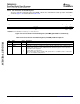
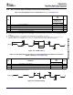
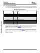
7.7.3.5 PLL Controller Divider 5 Register
The PLL controller divider 5 register (PLLDIV5) is shown in Figure 7-15 and described in Table 7-23 .
31 16
Reserved
R-0
15 14 5 4 0
D5EN Reserved RATIO
R/W-1 R-0 R/W-3
LEGEND: R/W = Read/Write; R = Read only; - n = value after reset
Figure 7-15. PLL Controller Divider 5 Register (PLLDIV5) [Hex Address: 029A 0164]
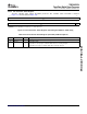
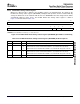
Table 7-23. PLL Controller Divider 5 Register (PLLDIV5) Field Descriptions
Bit Field Value Description
31:16 Reserved 0 Reserved. The reserved bit location is always read as 0. A value written to this field has no effect.
15 Dn4EN Divider 4 enable bit.
0 Divider 4 is disabled. No clock output.
1 Divider 4 is enabled.
14:5 Reserved 0 Reserved. The reserved bit location is always read as 0. A value written to this field has no effect.
4:0 RATIO 0-1Fh Divider ratio bits.
0 ÷1. Divide frequency by 1.
1h ÷2. Divide frequency by 2.
2h ÷3. Divide frequency by 3.
3h ÷4. Divide frequency by 4.
4h-7h ÷5 to ÷8. Divide frequency by 5 to divide frequency by 8.
8h-1Fh Reserved, do not use.
Submit Documentation Feedback C64x+ Peripheral Information and Electrical Specifications 131