
Memory Controller User's Guide

www.ti.com
4.13 DDR VTP Register (DDRVTPR)
4.14 DDR VTP Enable Register (DDRVTPER)
DDR2 Memory Controller Registers
The DDR VTP register (DDRVTPR) is used in conjunction with the VTP IO control register (VTPIOCR) to
calibrate the output impedance of the DDR2 memory controller IOs with respect to voltage, temperature,
and process. Following the calibration sequence, DDRVTPR contains the information needed to calibrate
the impedance of the IO. Once the calibration sequence has completed, DDRVTPR should be read and
the data written to the PCH and NCH fields in VTPIOCR. The DDRVTPR is shown in Figure 31 and
described in Table 37 .
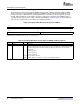
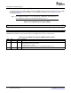
Figure 31. DDR VTP Register (DDRVTPR)
31 16
Reserved
R-0
15 10 9 5 4 0
Reserved PCH NCH
R-0 R-0 R/W-0
LEGEND: R/W = Read/Write; R = Read only; - n = value after reset
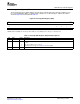
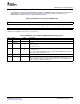
Table 37. DDR VTP Register (DDRVTPR) Field Descriptions
Bit Field Value Description
31-10 Reserved 0 Reserved.
9-5 PCH 0-1Fh P channel value for IO impedance calibration. Following the VTP calibration sequence, this value should
be read and written to the PCH field in the VTP IO control register (VTPIOCR).
4-0 NCH 0-1Fh N channel value for IO impedance calibration. Following the VTP calibration sequence, this value
should be read and written to the NCH field in the VTP IO control register (VTPIOCR).
The DDR VTP enable register (DDRVTPER) is used to enable/disable accesses to the DDR VTP register
(DDRVTPR). Writing a value of 1 to DDRVTPER enables accesses to DDRVTPR and writing a value of 0
disables accesses to DDRVTPR. The DDRVTPER is shown in Figure 32 and described in Table 38 .
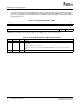
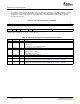
Figure 32. DDR VTP Enable Register (DDRVTPER)
31 16
Reserved
R-0
15 1 0
Reserved EN
R-0 R/W-0
LEGEND: R/W = Read/Write; R = Read only; - n = value after reset
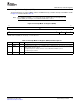
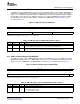
Table 38. DDR VTP Enable Register (DDRVTPER) Field Descriptions
Bit Field Value Description
31-1 Reserved 0 Reserved. Always write 0 to these bits.
0 EN DDRVTPR access enable.
0 Access to DDRVTPR is disabled.
1 Access to DDRVTPR is enabled.
SPRUEM4A – November 2007 DDR2 Memory Controller 55
Submit Documentation Feedback