
Memory Controller User's Guide

www.ti.com
DDR2 Memory Controller Registers
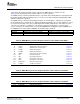
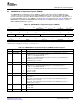
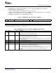
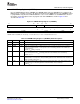
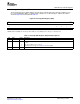
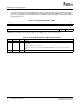
Table 26. SDRAM Bank Configuration Register (SDBCR) Field Descriptions (continued)
Bit Field Value Description
11-9 CL 0-7h CAS latency.
0-1h Reserved
2h CAS latency of 2
3h CAS latency of 3
4h CAS latency of 4
5h CAS latency of 5
6h-7h Reserved
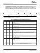
8-7 Reserved 0 Reserved
6-4 IBANK 0-7h Internal DDR2 bank setup. Defines the number of internal banks on the external DDR2 memory.
0 1 bank
1h 2 banks
2h 4 banks
3h 8 banks
4h-7h Reserved
3 Reserved 0 Reserved. Always write a 0 to this bit.
2-0 PAGESIZE 0-7h DDR2 page size. Defines the page size of each page of the external DDR2 memory.
0 256-word page requiring 8 column address bits.
1h 512-word page requiring 9 column address bits.
2h 1024-word page requiring 10 column address bits.
3h 2048-word page requiring 11 column address bits.
4h-7h Reserved
44 DDR2 Memory Controller SPRUEM4A – November 2007
Submit Documentation Feedback