
Memory Controller User's Guide

www.ti.com
3.2.4 Configuring DDR PHY Control Register (DDRPHYCR)
Supported Use Cases
The DDR PHY control register (DDRPHYCR) contains a read latency (READLAT) field that helps the
DDR2 memory controller determine when to sample read data. The READLAT field should be
programmed to a value equal to CAS latency plus round trip board delay minus 1. The minimum
READLAT value is CAS latency plus 1 and the maximum READLAT value is CAS latency plus 3 (again,
the READLAT field would be programmed to these values minus 1).
When calculating round trip board delay the signals of primary concern are the differential clock signals
(DDR_CLK and DDR_CLK) and data strobe signals (DDR_DQS). For these signals, calculate the round
trip board delay from the DDR2 memory controller to the memory and then choose the maximum delay to
determine the READLAT value. In this example we will assume the round trip board delay is 1 DDR_CLK
cycle, therefore READLAT can be calculated as follows:
READLAT = CAS latency + round trip board delay – 1 = 4 + 1 – 1 = 4
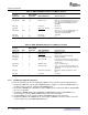
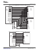
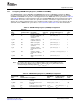
Table 21. DDR PHY Control Register (DDRPHYCR) Configuration
Register Field Name Description Register Value
DLLRESET Programmed to remove the DDR2 memory controller DLL from 0
reset.
DLLPWRDN Programmed to power up the DDR2 memory controller DLL. 0
READLAT Read latency is equal to CAS latency plus round trip board delay 4
for data minus 1.
40 DDR2 Memory Controller SPRUEM4A – November 2007
Submit Documentation Feedback