
Memory Controller User's Guide

www.ti.com
3.2.1 Configuring SDRAM Bank Configuration Register (SDBCR)
3.2.2 Configuring SDRAM Refresh Control Register (SDRCR)
Supported Use Cases
The SDRAM bank configuration register (SDBCR) contains register fields that configure the DDR2
memory controller to match the data bus width, CAS latency, number of banks, and page size of the
attached DDR2 memory. In this example, we assume the following configuration:
• Data bus width = 32 bits
• CAS latency = 4
• Number of banks = 8
• Page size = 1024 words
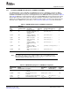
Table 16 shows the resulting SDBCR configuration. Note that the value of the TIMUNLOCK bit is
dependent on whether or not it is desirable to unlock SDTIMR and SDTIMR2. The TIMUNLOCK bit should
only be set to 1 when the SDTIMR and SDTIMR2 needs to be updated.
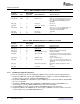
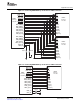
Table 16. SDRAM Bank Configuration Register (SDBCR) Configuration
Field Value Function Selection
TIMUNLOCK x Set to 1 to unlock the SDRAM timing register (SDTIMR) and the SDRAM timing register 2
(SDTIMR2). Cleared to 0 to lock SDTIMR and SDTIMR2.
NM 0h To configure the DDR2 memory controller for a 32-bit data bus width.
CL 4h To select a CAS latency of 4.
IBANK 3h To select 8 internal DDR2 banks.
PAGESIZE 2h To select 1024-word page size.
The SDRAM refresh control register (SDRCR) configures the DDR2 memory controller to meet the refresh
requirements of the attached DDR2 device. SDRCR also allows the DDR2 memory controller to enter and
exit self refresh and enable and disable the MCLK stopping. In this example, we assume that the DDR2
memory controller is not is in self-refresh mode and that MCLK stopping is disabled.
The RR bit field in SDRCR is defined as the rate at which the attached DDR2 device is refreshed in DDR2
cycles. The value of this field may be calculated using the following equation:
RR = DDR2 clock frequency × DDR2 refresh rate
Table 17 displays the DDR2-400 refresh rate specification.
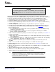
Table 17. DDR2 Memory Refresh Specification
Symbol Description Value
t
REF
Average Periodic Refresh Interval 7.8 µ s
Therefore, the following assumes a 133-MHZ DDR2 clock frequency:
RR = 133 MHZ × 7.8 µ s = 1037.4
Therefore, RR = 1038 = 40Eh.
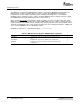
Table 18 shows the resulting SDRCR configuration.
Table 18. SDRAM Refresh Control Register (SDRCR) Configuration
Field Value Function Selection
SR 0 DDR2 memory controller is not in self-refresh mode.
MCLKSTOPEN 0 MCLK stopping is disabled.
RR 40Eh Set to 40Eh DDR2 clock cycles to meet the DDR2 memory refresh rate requirement.
DDR2 Memory Controller38 SPRUEM4A – November 2007
Submit Documentation Feedback