
Computer Hardware User's Guide

Timers
12-4
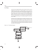
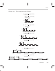
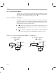
Figure 12–2. Memory-Mapped Timer Locations
Timer0 global control
†
Timer0 counter
‡
Timer0 period
‡
Timer1 global control
†
Timer1 counter
‡
Timer1 period
‡
808020h
808034h
808024h
808028h
808030h
808038h
‡
See Section 12.1.4
†
See Section 12.1.3
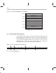
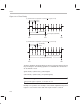
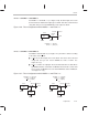
12.1.3 Timer Global-Control Register
The timer global-control register is a 32-bit register that contains the global and
port control bits for the timer module. Figure 12–3 shows the format of the
timer global-control register. Bits 3–0 are the port control bits; bits
11–6 are the timer global-control bits. At reset, all bits are set to 0 except for
DATIN (which is set to the value read on TCLK). Table 12–1 describes the
timer global-control register bits, their names, and functions.
Figure 12–3. Timer Global-Control Register
31 16 15 12 11 10 9 8 7 6 5 4 3 2 1 0
xx xx TSTAT INV CLKSRC C/P HLD GO xx xx DATIN DATOUT I/O FUNC
R R/W R/W R/W R/W R/W R R/W R/W R/W
Notes: 1) R = read, W = write
2) xx = reserved bit, read as 0