
Computer Hardware User's Guide

Programmable Bank Switching
10-17
TMS320C32 Enhanced External Memory Interface
10.5 Programmable Bank Switching
Programmable bank switching allows you to switch between external memory
banks without having to insert wait states externally due to memories that require
several cycles to turn off. Bank switching is implemented on STRB0 and STRB1
only.
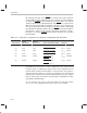
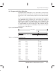
The size of a bank is determined by the number of bits specified to be examined
on the BNKCMP field of the primary bus control register. For example, if
BNKCMP = 16, the 16 MSBs of the address are used to define a bank (see
Figure 9–4). Since addresses are 24 bits, the bank size is specified by the eight
LSBs, yielding a bank size of 256 words. If BNKCMP ≥ 16, only the 16 MSBs
are compared. Bank sizes from 2
8
= 256 to 2
24
= 16M are allowed. Table 9–6
summarizes the relationship between BNKCMP, the address bits used to define
a bank, and the resulting bank size.
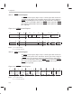
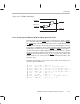
Figure 10–8. BNKCMP Example
23 8 7 0
24-bit address
Number of bits to compare
Defines bank size
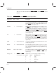
Table 10–4. BNKCMP and Bank Size
BNKCMP MSBs Defining a Bank Bank Size (32-Bit Words)
00000 None 2
24 =
16M
00001 23 2
23
=8M
00010 23–22 2
22
=4M
00011 23–21 2
21
=2M
00100 23–20 2
20
=1M
00101 23–19 2
19
= 512K
00110 23–18 2
18
= 256K
00111 23–17 2
17
= 128K
01000 23–16 2
16
= 64K
01001 23–15 2
15
= 32K
01010 23–14 2
14
= 16K
01011 23–13 2
13
=8K
01100 23–12 2
12
=4K
01101 23–11 2
11
=2K
01110 23–10 2
10
=1K
01111 23–9 2
9
= 512
10000 23–8 2
8
= 256
10001–11111
Reserved Undefined