
Computer Hardware User's Guide

Configuration
10-14
By setting the bit fields of the STRB0 bus control register with a physical-
memory width of 32 bits and a data type size of 32 bits, the external address
referring to the STRB0
location is identical to the internal address used by the
‘C32 CPU. Alternatively, setting the bit fields of the STRB1 bus control register
with a physical memory width of 16-bit and a data-type size of 16-bit, the ad-
dress presented by the ‘C32 external pins is the internal address shifted right
by one bit with A
23
driving A
23
and A
22
. Since the STRB1 memory-bank address
pins A
23
A
22
A
21
...A
1
A
0
are connected to the ‘C32 address pins A
22
A
21
...A
1
A
0
A
–1
,
the address seen by the STRB1 memory bank is identical to the ‘C32 CPU
internal address.
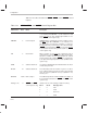
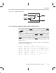
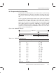
Table 10–2. Data-Access Sequence for a Memory Configuration with Two Banks
Instruction #
Internal
Address Bus
External
Address Pins
Active Strobe Byte Enable
Accessed
Data Pins
(2)
4000h 4000h STRB0_B0/B1/B2/B3
D
31–0
4000h
(3)
4001h 4001h STRB0_B0/B1/B2/B3
D
31–0
4001h
(4)
4002h 4002h STRB0_B0/B1/B2/B3
D
31–0
4002h
(5)
4003h 4003h STRB0_B0/B1/B2/B3
D
31–0
4003h
(8)
900000h C80000h STRB1_B0/B1 and
STRB1_B3
/A
–1
= 0
D
15–0
900000h
(9)
900001h C80001h STRB1_B0/B1 and
D
15–0
900001h
STRB1_B3/A
–1
= 1
The ability of the ‘C32 device to select a single byte from a single external
memory location or combinations of bytes from several contiguous memory
locations dictates that the internal address seen by the CPU correspond to a
shifted version of the address presented to the external pins. The ’C32 external
memory interface handles this conversion automatically as long as you configure
the bus control register to match the external memory configuration present in
your hardware implementation.
As seen in Figure 2–8 on page 2-20, ’C32 handles nine different memory
access cases. The following sections discuss these cases in detail.