
Computer Hardware User's Guide

Configuration
10-8
10.3.1.1 STRB0 Control Register
The STRB0 control register (Figure 10–4) is a 32-bit register that contains the
control bits for the portion of the external bus memory space that is mapped to
STRB0. The following table lists the register bits with the bit names and functions.
At the system reset, 0F10F8h is written to the STRB0
control register if the PRGW
pin is logic low and 0710F8h is written to the STRB0 control register if the PRGW
pin is logic high.
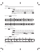
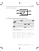
Figure 10–4. STRB0 Control Register
31 28
27 24 23
22 21 20 19 18 17 16
xx
STRB
switch
STRB
config
Sign ext/
zero fill
Physical memory
width
Data type size
R/W R/W R/W R/W R/W R/W R/W
15 13 12 11 8 7 5 4 3 2 1 0
xx BNKCMP WTCNT SWW HIZ NOHOLD HOLDST
R/W R/W R/W R/W R/W R
Notes: 1) R = read, W = write
2) xx = reserved, read as 0
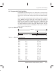
10.3.1.2 STRB1 Control Register
The STRB1 control register (Figure 10–5) is a 32-bit register that contains the
control bits for the portion of the external bus memory space that is mapped
to STRB1
. Figure 10–5 shows the register bits with their names and functions.
At system reset, 0F10F8h is written to the STRB1 control register if the PRGW
pin is logic low and 0710F8h is written to the STRB1 control register if the
PRGW pin is logic high.
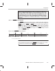
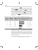
Figure 10–5. STRB1 Control Register
31 24 23 21 20 19 18 17 16 15 13 12 8 7 5 4 3 2 0
xx xx
Sign ext/
zero fill
Physical
memory
width
Data-
type
size
xx BNKCMP WTCNT SWW xx
R/W R/W R/W R/W R/W R/W R/W
Notes: 1) R = read, W = write
2) xx = reserved, read as 0