
Computer Hardware User's Guide

Decode/address
generation held
until AR is read
ARs read
Pipeline Conflicts
8-8
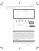
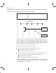
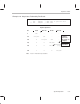
In Example 8–4, two auxiliary registers are added together, with the result going
to an extended-precision register. The next instruction uses a different auxiliary
register as an address register.
Example 8–4. A Read of ARs Followed by ARs for Address Generation
ADDI AR0,AR1,R1 ; AR0+AR1 → R1
NEXT MPYF *++AR2,R0 ; Decode delayed one cycle
ADDF
FLOAT
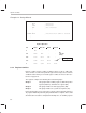
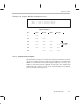
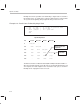
Pipeline Operation
PC Fetch
Decode Read Execute
n ADDI — — —
n+1 MPYF ADDI — —
n+2 ADDF MPYF ADDI —
n+2 ADDF MYPF (nop) ADDI AR0,AR1,R0
n+3 FLOAT ADDF MPYF (nop)
Note:
Loop counter auxiliary registers for the decrement and branch (DBR) instruc-
tions are regarded in the same way as they are for addressing. The operation
shown in Example 8–3 and Example 8–4 also can occur for this instruction.
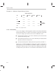
8.2.3 Memory Conflicts
Memory conflicts can occur when the memory bandwidth of a physical memory
space is exceeded. For example, RAM blocks 0 and 1 and the ROM block can
support only two accesses per cycle. The external interface can support only
one access per cycle. Section 8.4,
Memory Access for Maximum Performance
,
on page 8-22 contains some conditions under which you can avoid memory
conflicts.