
Computer Hardware User's Guide

Interrupts
7-36
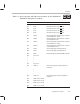
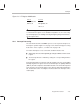
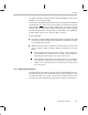
Table 7–8. Interrupt Latency
Cycle Description Fetch Decode Read Execute
1 Recognize interrupt in single-cycle fetched
(prog a + 1) instruction
prog a + 1 prog a prog a–1 prog a–2
2 Clear GIE bit. Clear interrupt flag — interrupt prog a prog a–1
3 Read the interrupt vector table — — interrupt prog a
4 Store return address to stack — — — interrupt
5 Pipeline begins to fill with ISR instruction isr1 — — —
6 Pipeline continues to fill with ISR instruction isr2 isr1 — —
7 Pipeline continues to fill with ISR instruction isr3 isr2 isr1 —
8
Execute first instruction of interrupt service routine isr4 isr3 isr2 isr1
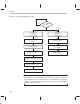
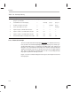
7.6.8 External Interrupts
The four external maskable interrupt pins INT0–INT3 are enabled at the IF reg-
ister (Section 3.1.9,
CPU Interrupt Flag (IF) Register
, on page 3-11) and are syn-
chronized internally. They are sampled on the falling edge of H1 and passed
through a series of H1/H3 latches internally. These latches require the interrupt
signal to be held low for at least one H1/H3 clock cycle to be recognized by the
‘C3x. Once synchronized, the interrupt input sets the corresponding interrupt
flag register (IF) bit if the interrupt is active.
Figure 7–7 shows a functional diagram of the logic used to implement external
interrupt inputs.