
Calculator User Manual
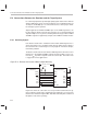
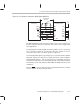
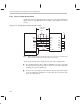
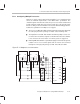
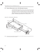
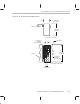
Table Of Contents
- Read This First
- Contents
- Figures
- Tables
- Examples
- Cautions
- Introduction
- Architectural Overview
- Central Processing Unit
- Memory and I/O Spaces
- Program Control
- Addressing Modes
- Assembly Language Instructions
- Instruction Set Summary
- How To Use the Instruction Descriptions
- Instruction Descriptions
- ABS
- ABS
- ADD
- ADD
- ADD
- ADD
- ADDC
- ADDC
- ADDS
- ADDS
- ADDT
- ADDT
- ADRK
- AND
- AND
- AND
- APAC
- APAC
- B
- BACC
- BANZ
- BANZ
- BCND
- BCND
- BIT
- BIT
- BITT
- BITT
- BLDD
- BLDD
- BLDD
- BLDD
- BLDD
- BLPD
- BLPD
- BLPD
- BLPD
- CALA
- CALL
- CC
- CC
- CLRC
- CLRC
- CMPL
- CMPR
- DMOV
- DMOV
- IDLE
- IN
- IN
- INTR
- LACC
- LACC
- LACC
- LACL
- LACL
- LACL
- LACT
- LACT
- LAR
- LAR
- LAR
- LDP
- LDP
- LPH
- LPH
- LST
- LST
- LST
- LST
- LT
- LT
- LTA
- LTA
- LTD
- LTD
- LTD
- LTP
- LTP
- LTS
- LTS
- MAC
- MAC
- MAC
- MAC
- MACD
- MACD
- MACD
- MACD
- MACD
- MAR
- MAR
- MPY
- MPY
- MPY
- MPYA
- MPYA
- MPYS
- MPYS
- MPYU
- MPYU
- NEG
- NEG
- NMI
- NOP
- NORM
- NORM
- NORM
- OR
- OR
- OR
- OUT
- OUT
- PAC
- POP
- POP
- POPD
- POPD
- PSHD
- PSHD
- PUSH
- RET
- RETC
- ROL
- ROR
- RPT
- RPT
- SACH
- SACH
- SACL
- SACL
- SAR
- SAR
- SBRK
- SETC
- SETC
- SFL
- SFR
- SFR
- SPAC
- SPH
- SPH
- SPL
- SPL
- SPLK
- SPLK
- SPM
- SQRA
- SQRA
- SQRS
- SQRS
- SST
- SST
- SUB
- SUB
- SUB
- SUB
- SUBB
- SUBB
- SUBC
- SUBC
- SUBS
- SUBS
- SUBT
- SUBT
- TBLR
- TBLR
- TBLR
- TBLW
- TBLW
- TBLW
- TRAP
- XOR
- XOR
- XOR
- ZALR
- ZALR
- On-Chip Peripherals
- Synchronous Serial Port
- Asynchronous Serial Port
- TMS320C209
- Register Summary
- TMS320C1x/C2x/C2xx/C5x Instruction Set Comparison
- Program Examples
- Submitting ROM Codes to TI
- Design Considerations for Using XDS510 Emulator
- E.1 Designing Your Target System’s Emulator Connector (14-Pin Header)
- E.2 Bus Protocol
- E.3 Emulator Cable Pod
- E.4 Emulator Cable Pod Signal Timing
- E.5 Emulation Timing Calculations
- E.6 Connections Between the Emulator and the Target System
- E.7 Physical Dimensions for the 14-Pin Emulator Connector
- E.8 Emulation Design Considerations
- Glossary
- Index

Emulation Design Considerations
E-18
E.8.2 Emulation Timing Calculations for a Scan Path Linker (SPL)
Example E–3 and Example E–4 help you to calculate the key emulation tim-
ings in the SPL secondary scan path of your system. For actual target timing
parameters, see the appropriate device data sheet for your target device.
The examples use the following assumptions:
t
su(TTMS)
Setup time, target TMS/TDI to TCK high 10 ns
t
d(TTDO)
Delay time, target TDO from TCK low 15 ns
t
d(bufmax)
Delay time, target buffer, maximum 10 ns
t
d(bufmin)
Delay time, target buffer, minimum 1 ns
t
(bufskew)
Skew time, target buffer, between two
devices in the same package:
[t
d(bufmax)
– t
d(bufmin)
] × 0.15
1.35 ns
t
(TCKfactor)
Duty cycle, TCK assume a 40/60% clock 0.4
(40%)
Also, the examples use the following values from the SPL data sheet:
t
d(DTMSmax)
Delay time, SPL DTMS/DTDO from TCK
low, maximum
31 ns
t
su(DTDLmin)
Setup time, DTDI to SPL TCK high,
minimum
7 ns
t
d(DTCKHmin)
Delay time, SPL DTCK from TCK high,
minimum
2 ns
t
d(DTCKLmax)
Delay time, SPL DTCK from TCK low,
maximum
16 ns
There are two key timing paths to consider in the emulation design:
The TCK-to-DTMS/DTDO path, called t
pd(TCK-DTMS)
The TCK-to-DTDI path, called t
pd(TCK-DTDI)