
Calculator User Manual
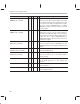
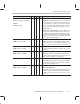
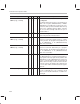
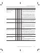
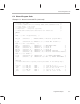
Table Of Contents
- Read This First
- Contents
- Figures
- Tables
- Examples
- Cautions
- Introduction
- Architectural Overview
- Central Processing Unit
- Memory and I/O Spaces
- Program Control
- Addressing Modes
- Assembly Language Instructions
- Instruction Set Summary
- How To Use the Instruction Descriptions
- Instruction Descriptions
- ABS
- ABS
- ADD
- ADD
- ADD
- ADD
- ADDC
- ADDC
- ADDS
- ADDS
- ADDT
- ADDT
- ADRK
- AND
- AND
- AND
- APAC
- APAC
- B
- BACC
- BANZ
- BANZ
- BCND
- BCND
- BIT
- BIT
- BITT
- BITT
- BLDD
- BLDD
- BLDD
- BLDD
- BLDD
- BLPD
- BLPD
- BLPD
- BLPD
- CALA
- CALL
- CC
- CC
- CLRC
- CLRC
- CMPL
- CMPR
- DMOV
- DMOV
- IDLE
- IN
- IN
- INTR
- LACC
- LACC
- LACC
- LACL
- LACL
- LACL
- LACT
- LACT
- LAR
- LAR
- LAR
- LDP
- LDP
- LPH
- LPH
- LST
- LST
- LST
- LST
- LT
- LT
- LTA
- LTA
- LTD
- LTD
- LTD
- LTP
- LTP
- LTS
- LTS
- MAC
- MAC
- MAC
- MAC
- MACD
- MACD
- MACD
- MACD
- MACD
- MAR
- MAR
- MPY
- MPY
- MPY
- MPYA
- MPYA
- MPYS
- MPYS
- MPYU
- MPYU
- NEG
- NEG
- NMI
- NOP
- NORM
- NORM
- NORM
- OR
- OR
- OR
- OUT
- OUT
- PAC
- POP
- POP
- POPD
- POPD
- PSHD
- PSHD
- PUSH
- RET
- RETC
- ROL
- ROR
- RPT
- RPT
- SACH
- SACH
- SACL
- SACL
- SAR
- SAR
- SBRK
- SETC
- SETC
- SFL
- SFR
- SFR
- SPAC
- SPH
- SPH
- SPL
- SPL
- SPLK
- SPLK
- SPM
- SQRA
- SQRA
- SQRS
- SQRS
- SST
- SST
- SUB
- SUB
- SUB
- SUB
- SUBB
- SUBB
- SUBC
- SUBC
- SUBS
- SUBS
- SUBT
- SUBT
- TBLR
- TBLR
- TBLR
- TBLW
- TBLW
- TBLW
- TRAP
- XOR
- XOR
- XOR
- ZALR
- ZALR
- On-Chip Peripherals
- Synchronous Serial Port
- Asynchronous Serial Port
- TMS320C209
- Register Summary
- TMS320C1x/C2x/C2xx/C5x Instruction Set Comparison
- Program Examples
- Submitting ROM Codes to TI
- Design Considerations for Using XDS510 Emulator
- E.1 Designing Your Target System’s Emulator Connector (14-Pin Header)
- E.2 Bus Protocol
- E.3 Emulator Cable Pod
- E.4 Emulator Cable Pod Signal Timing
- E.5 Emulation Timing Calculations
- E.6 Connections Between the Emulator and the Target System
- E.7 Physical Dimensions for the 14-Pin Emulator Connector
- E.8 Emulation Design Considerations
- Glossary
- Index

Instruction Set Comparison Table
B-34
Syntax
Description5x2xx2x1x
SUBT
dma
SUBT {
ind
} [
, next ARP
]
√
√
√
√
√
√
Subtract From Accumulator With Shift Specified
by T Register
Left shift the data-memory value as specified by the 4
LSBs of the T register (TMS320C2x/2xx) or TREG1
(TMS320C5x), and subtract the result from the accu-
mulator. If a shift is specified, left shift the data-memory
value before subtracting. During shifting, low-order
bits are zero filled, and high-order bits are sign ex-
tended if SXM = 1.
SXF
√ √ √
Set External Flag
Set the XF pin and the XF status bit to 1.
TBLR
dma
TBLR {
ind
} [
, next ARP
]
√
√
√
√
√
√
√
√
Table Read
Transfer a word from program memory to a data-
memory location. The program-memory address is in
the 12 (TMS320C1x) or 16 (TMS320C2x/2xx/5x)
LSBs of the accumulator.
TBLW
dma
TBLW {
ind
} [
, next ARP
]
√
√
√
√
√
√
√
√
Table Write
Transfer a word from data-memory to a program-
memory location. The program-memory address is in
the 12 (TMS320C1x) or 16 (TMS320C2x/2xx/5x)
LSBs of the accumulator.
TRAP
√ √ √
Software Interrupt
The TRAP instruction is a software interrupt that trans-
fers program control to program-memory address 30h
(TMS320C2x) or 22h (TMS320C2xx/5x) and pushes
the PC + 1 onto the hardware stack. The instruction at
address 30h or 22h may contain a branch instruction
to transfer control to the TRAP routine. Putting the PC
+ 1 on the stack enables an RET instruction to pop the
return PC.
XC
n, cond
1
[
, cond
2
] [, ...]
√
Execute Conditionally
Execute conditionally the next
n
instruction words
where 1
≤
n
≤ 2. Not all combinations of conditions are
meaningful.