
Calculator User Manual
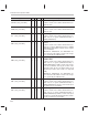
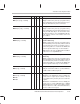
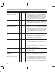
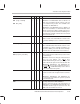
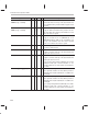
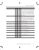
Table Of Contents
- Read This First
- Contents
- Figures
- Tables
- Examples
- Cautions
- Introduction
- Architectural Overview
- Central Processing Unit
- Memory and I/O Spaces
- Program Control
- Addressing Modes
- Assembly Language Instructions
- Instruction Set Summary
- How To Use the Instruction Descriptions
- Instruction Descriptions
- ABS
- ABS
- ADD
- ADD
- ADD
- ADD
- ADDC
- ADDC
- ADDS
- ADDS
- ADDT
- ADDT
- ADRK
- AND
- AND
- AND
- APAC
- APAC
- B
- BACC
- BANZ
- BANZ
- BCND
- BCND
- BIT
- BIT
- BITT
- BITT
- BLDD
- BLDD
- BLDD
- BLDD
- BLDD
- BLPD
- BLPD
- BLPD
- BLPD
- CALA
- CALL
- CC
- CC
- CLRC
- CLRC
- CMPL
- CMPR
- DMOV
- DMOV
- IDLE
- IN
- IN
- INTR
- LACC
- LACC
- LACC
- LACL
- LACL
- LACL
- LACT
- LACT
- LAR
- LAR
- LAR
- LDP
- LDP
- LPH
- LPH
- LST
- LST
- LST
- LST
- LT
- LT
- LTA
- LTA
- LTD
- LTD
- LTD
- LTP
- LTP
- LTS
- LTS
- MAC
- MAC
- MAC
- MAC
- MACD
- MACD
- MACD
- MACD
- MACD
- MAR
- MAR
- MPY
- MPY
- MPY
- MPYA
- MPYA
- MPYS
- MPYS
- MPYU
- MPYU
- NEG
- NEG
- NMI
- NOP
- NORM
- NORM
- NORM
- OR
- OR
- OR
- OUT
- OUT
- PAC
- POP
- POP
- POPD
- POPD
- PSHD
- PSHD
- PUSH
- RET
- RETC
- ROL
- ROR
- RPT
- RPT
- SACH
- SACH
- SACL
- SACL
- SAR
- SAR
- SBRK
- SETC
- SETC
- SFL
- SFR
- SFR
- SPAC
- SPH
- SPH
- SPL
- SPL
- SPLK
- SPLK
- SPM
- SQRA
- SQRA
- SQRS
- SQRS
- SST
- SST
- SUB
- SUB
- SUB
- SUB
- SUBB
- SUBB
- SUBC
- SUBC
- SUBS
- SUBS
- SUBT
- SUBT
- TBLR
- TBLR
- TBLR
- TBLW
- TBLW
- TBLW
- TRAP
- XOR
- XOR
- XOR
- ZALR
- ZALR
- On-Chip Peripherals
- Synchronous Serial Port
- Asynchronous Serial Port
- TMS320C209
- Register Summary
- TMS320C1x/C2x/C2xx/C5x Instruction Set Comparison
- Program Examples
- Submitting ROM Codes to TI
- Design Considerations for Using XDS510 Emulator
- E.1 Designing Your Target System’s Emulator Connector (14-Pin Header)
- E.2 Bus Protocol
- E.3 Emulator Cable Pod
- E.4 Emulator Cable Pod Signal Timing
- E.5 Emulation Timing Calculations
- E.6 Connections Between the Emulator and the Target System
- E.7 Physical Dimensions for the 14-Pin Emulator Connector
- E.8 Emulation Design Considerations
- Glossary
- Index

Instruction Set Comparison Table
B-27
TMS320C1x/C2x/C2xx/C5x Instruction Set Comparison
Syntax
Description5x2xx2x1x
RETE
√
Enable Interrupts and Return From Interrupt
Copy the contents of the top of the stack into the PC
and pop the stack one level. RETE automatically
clears the global interrupt enable bit and pops the
shadow registers (stored when the interrupt was tak-
en) back into their corresponding strategic registers.
The following registers are shadowed: ACC, ACCB,
PREG, ST0, ST1, PMST, ARCR, INDX, TREG0,
TREG1, TREG2.
RETI
√
Return From Interrupt
Copy the contents of the top of the stack into the PC
and pop the stack one level. RETI also pops the values
in the shadow registers (stored when the interrupt was
taken) back into their corresponding strategic regis-
ters. The following registers are shadowed: ACC,
ACCB, PREG, ST0, ST1, PMST, ARCR, INDX,
TREG0, TREG1, TREG2.
RFSM
√
Reset Serial Port Frame Synchronization Mode
Reset the FSM status bit to 0.
RHM
√ √
Reset Hold Mode
Reset the HM status bit to 0.
ROL
√ √ √
Rotate Accumulator Left
Rotate the accumulator left one bit.
ROLB
√
Rotate ACCB and Accumulator Left
Rotate the ACCB and the accumulator left by one bit;
this results in a 65-bit rotation.
ROR
√ √ √
Rotate Accumulator Right
Rotate the accumulator right one bit.
RORB
√
Rotate ACCB and Accumulator Right
Rotate the ACCB and the accumulator right one bit;
this results in a 65-bit rotation.
ROVM
√ √ √ √
Reset Overflow Mode
Reset the OVM status bit to 0; this disables overflow
mode.