
Calculator User Manual
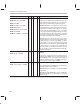
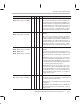
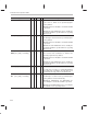
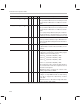
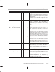
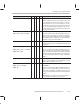
Table Of Contents
- Read This First
- Contents
- Figures
- Tables
- Examples
- Cautions
- Introduction
- Architectural Overview
- Central Processing Unit
- Memory and I/O Spaces
- Program Control
- Addressing Modes
- Assembly Language Instructions
- Instruction Set Summary
- How To Use the Instruction Descriptions
- Instruction Descriptions
- ABS
- ABS
- ADD
- ADD
- ADD
- ADD
- ADDC
- ADDC
- ADDS
- ADDS
- ADDT
- ADDT
- ADRK
- AND
- AND
- AND
- APAC
- APAC
- B
- BACC
- BANZ
- BANZ
- BCND
- BCND
- BIT
- BIT
- BITT
- BITT
- BLDD
- BLDD
- BLDD
- BLDD
- BLDD
- BLPD
- BLPD
- BLPD
- BLPD
- CALA
- CALL
- CC
- CC
- CLRC
- CLRC
- CMPL
- CMPR
- DMOV
- DMOV
- IDLE
- IN
- IN
- INTR
- LACC
- LACC
- LACC
- LACL
- LACL
- LACL
- LACT
- LACT
- LAR
- LAR
- LAR
- LDP
- LDP
- LPH
- LPH
- LST
- LST
- LST
- LST
- LT
- LT
- LTA
- LTA
- LTD
- LTD
- LTD
- LTP
- LTP
- LTS
- LTS
- MAC
- MAC
- MAC
- MAC
- MACD
- MACD
- MACD
- MACD
- MACD
- MAR
- MAR
- MPY
- MPY
- MPY
- MPYA
- MPYA
- MPYS
- MPYS
- MPYU
- MPYU
- NEG
- NEG
- NMI
- NOP
- NORM
- NORM
- NORM
- OR
- OR
- OR
- OUT
- OUT
- PAC
- POP
- POP
- POPD
- POPD
- PSHD
- PSHD
- PUSH
- RET
- RETC
- ROL
- ROR
- RPT
- RPT
- SACH
- SACH
- SACL
- SACL
- SAR
- SAR
- SBRK
- SETC
- SETC
- SFL
- SFR
- SFR
- SPAC
- SPH
- SPH
- SPL
- SPL
- SPLK
- SPLK
- SPM
- SQRA
- SQRA
- SQRS
- SQRS
- SST
- SST
- SUB
- SUB
- SUB
- SUB
- SUBB
- SUBB
- SUBC
- SUBC
- SUBS
- SUBS
- SUBT
- SUBT
- TBLR
- TBLR
- TBLR
- TBLW
- TBLW
- TBLW
- TRAP
- XOR
- XOR
- XOR
- ZALR
- ZALR
- On-Chip Peripherals
- Synchronous Serial Port
- Asynchronous Serial Port
- TMS320C209
- Register Summary
- TMS320C1x/C2x/C2xx/C5x Instruction Set Comparison
- Program Examples
- Submitting ROM Codes to TI
- Design Considerations for Using XDS510 Emulator
- E.1 Designing Your Target System’s Emulator Connector (14-Pin Header)
- E.2 Bus Protocol
- E.3 Emulator Cable Pod
- E.4 Emulator Cable Pod Signal Timing
- E.5 Emulation Timing Calculations
- E.6 Connections Between the Emulator and the Target System
- E.7 Physical Dimensions for the 14-Pin Emulator Connector
- E.8 Emulation Design Considerations
- Glossary
- Index

Instruction Set Comparison Table
B-16
Syntax
Description5x2xx2x1x
CC
pma,
cond
1
[
, cond
2
] [, ...]
√
Call Conditionally
If the specified conditions are met, control is passed to
the pma. Not all combinations of conditions are mean-
ingful.
CC[
D
]
pma
,
cond
1
[
, cond
2
] [, ...]
√
Call Conditionally With Optional Delay
If the specified conditions are met, control is passed to
the pma. Not all combinations of conditions are mean-
ingful.
If you specify a delayed branch (CCD), the next two in-
struction words (two 1-word instructions or one 2-word
instruction) are fetched and executed before the call.
CLRC
control bit
√ √
Clear Control Bit
Set the specified control bit to a logic 0. Maskable inter-
rupts are enabled immediately after the CLRC instruc-
tion executes.
CMPL
√ √ √
Complement Accumulator
Complement the contents of the accumulator (1s com-
plement).
CMPR
CM
√ √ √
Compare Auxiliary Register With AR0
Compare the contents of the current auxiliary register
to AR0, based on the following cases:
If CM = 00
2
, test whether AR(ARP) = AR0.
If CM = 01
2
, test whether AR(ARP) < AR0.
If CM = 10
2
, test whether AR(ARP) > AR0.
If CM = 11
2
, test whether AR(ARP) ≠ AR0.
If the result is true, load a 1 into the TC status bit; other-
wise, load a 0 into the TC bit. The comparison does not
affect the tested registers.
TMS320C5x devices: Compare the contents of the
auxiliary register with the ARCR.
CNFD
√ √ √
Configure Block as Data Memory
Configure on-chip RAM block B0 as data memory.
Block B0 is mapped into data-memory locations
512h–767h.
TMS320C5x devices: Block B0 is mapped into data-
memory locations 512h–1023h.