
Calculator User Manual
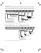
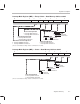
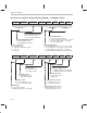
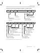
Table Of Contents
- Read This First
- Contents
- Figures
- Tables
- Examples
- Cautions
- Introduction
- Architectural Overview
- Central Processing Unit
- Memory and I/O Spaces
- Program Control
- Addressing Modes
- Assembly Language Instructions
- Instruction Set Summary
- How To Use the Instruction Descriptions
- Instruction Descriptions
- ABS
- ABS
- ADD
- ADD
- ADD
- ADD
- ADDC
- ADDC
- ADDS
- ADDS
- ADDT
- ADDT
- ADRK
- AND
- AND
- AND
- APAC
- APAC
- B
- BACC
- BANZ
- BANZ
- BCND
- BCND
- BIT
- BIT
- BITT
- BITT
- BLDD
- BLDD
- BLDD
- BLDD
- BLDD
- BLPD
- BLPD
- BLPD
- BLPD
- CALA
- CALL
- CC
- CC
- CLRC
- CLRC
- CMPL
- CMPR
- DMOV
- DMOV
- IDLE
- IN
- IN
- INTR
- LACC
- LACC
- LACC
- LACL
- LACL
- LACL
- LACT
- LACT
- LAR
- LAR
- LAR
- LDP
- LDP
- LPH
- LPH
- LST
- LST
- LST
- LST
- LT
- LT
- LTA
- LTA
- LTD
- LTD
- LTD
- LTP
- LTP
- LTS
- LTS
- MAC
- MAC
- MAC
- MAC
- MACD
- MACD
- MACD
- MACD
- MACD
- MAR
- MAR
- MPY
- MPY
- MPY
- MPYA
- MPYA
- MPYS
- MPYS
- MPYU
- MPYU
- NEG
- NEG
- NMI
- NOP
- NORM
- NORM
- NORM
- OR
- OR
- OR
- OUT
- OUT
- PAC
- POP
- POP
- POPD
- POPD
- PSHD
- PSHD
- PUSH
- RET
- RETC
- ROL
- ROR
- RPT
- RPT
- SACH
- SACH
- SACL
- SACL
- SAR
- SAR
- SBRK
- SETC
- SETC
- SFL
- SFR
- SFR
- SPAC
- SPH
- SPH
- SPL
- SPL
- SPLK
- SPLK
- SPM
- SQRA
- SQRA
- SQRS
- SQRS
- SST
- SST
- SUB
- SUB
- SUB
- SUB
- SUBB
- SUBB
- SUBC
- SUBC
- SUBS
- SUBS
- SUBT
- SUBT
- TBLR
- TBLR
- TBLR
- TBLW
- TBLW
- TBLW
- TRAP
- XOR
- XOR
- XOR
- ZALR
- ZALR
- On-Chip Peripherals
- Synchronous Serial Port
- Asynchronous Serial Port
- TMS320C209
- Register Summary
- TMS320C1x/C2x/C2xx/C5x Instruction Set Comparison
- Program Examples
- Submitting ROM Codes to TI
- Design Considerations for Using XDS510 Emulator
- E.1 Designing Your Target System’s Emulator Connector (14-Pin Header)
- E.2 Bus Protocol
- E.3 Emulator Cable Pod
- E.4 Emulator Cable Pod Signal Timing
- E.5 Emulation Timing Calculations
- E.6 Connections Between the Emulator and the Target System
- E.7 Physical Dimensions for the 14-Pin Emulator Connector
- E.8 Emulation Design Considerations
- Glossary
- Index
Register Descriptions
A-14
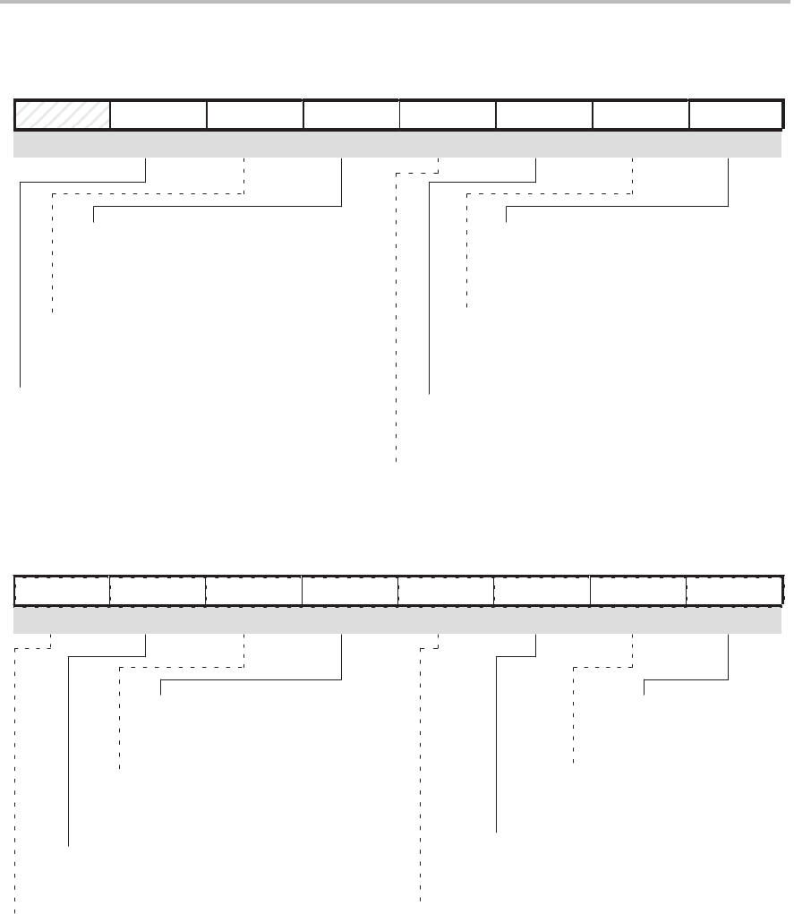
I/O Status Register (IOSR) — I/O Address FFF6h
15 14 13 12 11 10 9 8
0 0 0 1 1 0 0 0
Reserved
†
ADC
‡
BI
‡
TEMT THRE
‡
FE
‡
OE
‡
DR
‡
RR/W1C R/W1C
0
1
Normal operation.
CAD bit of ASPCR is 1 and
A
or
a
is received in ADTR.
0
1
Normal operation
Break has been detected on RX pin.
0
1
ADTR and/or AXSR are full.
ADTR and AXSR are empty; ADTR is
ready for a new character to transmit.
0
1
Transmit register not empty. Port operation normal.
Transmit register empty. Port ready to receive new
character.
0
1
No framing error detected.
Character received did not have a valid stop bit.
0
1
No overrun error detected.
Last character in ADTR was not read
before the next character overwrote it.
0
1
Receive register empty
Character has been completely
received.
A
detect complete bit
Break interrupt indicator
Transmit empty indicator
Transmit register empty indicator
Data ready indicator for receiver
Framing error indicator
Receive register overrun indicator
R/W1C R R/W1C R
7 6 5 4 3 2 1 0
X X X X X X X X
DIO3
‡
DIO2
‡
DIO1
‡
DIO0
‡
IO3
§
IO2
§
IO1
§
IO0
§
R/WR/W1C R/W1C
0
1
No change detected on IO2
Change detected on IO2
0
1
No change detected on IO1
Change detected on IO1
0
1
No change detected on IO0
Change detected on IO0
0
1
IO3 signal low
IO3 signal high
0
1
IO2 signal low
IO2 signal high
0
1
IO1 signal low
IO1 signal high
0
1
IO0 signal low
IO0 signal high
Change detect bit for IO2
Change detect bit for IO1
Change detect bit for IO0
IO3 pin status
IO0 pin status
IO2 pin status
IO1 pin status
0
1
No change detected on IO3
Change detected on IO3
Change detect bit for IO3
R/W1C R/W1C R/W R/W R/W
†
This reserved bit is always read as 0. Writes have no effect.
‡
When any one of these bits changes in response to the specified event, an interrupt request is generated on the TXRXINT line.
§
This bit can be written to only when the corresponding pin is configured (in the ASPCR) as an output.