
Calculator User Manual
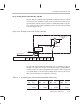
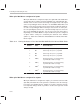
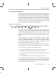
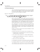
Table Of Contents
- Read This First
- Contents
- Figures
- Tables
- Examples
- Cautions
- Introduction
- Architectural Overview
- Central Processing Unit
- Memory and I/O Spaces
- Program Control
- Addressing Modes
- Assembly Language Instructions
- Instruction Set Summary
- How To Use the Instruction Descriptions
- Instruction Descriptions
- ABS
- ABS
- ADD
- ADD
- ADD
- ADD
- ADDC
- ADDC
- ADDS
- ADDS
- ADDT
- ADDT
- ADRK
- AND
- AND
- AND
- APAC
- APAC
- B
- BACC
- BANZ
- BANZ
- BCND
- BCND
- BIT
- BIT
- BITT
- BITT
- BLDD
- BLDD
- BLDD
- BLDD
- BLDD
- BLPD
- BLPD
- BLPD
- BLPD
- CALA
- CALL
- CC
- CC
- CLRC
- CLRC
- CMPL
- CMPR
- DMOV
- DMOV
- IDLE
- IN
- IN
- INTR
- LACC
- LACC
- LACC
- LACL
- LACL
- LACL
- LACT
- LACT
- LAR
- LAR
- LAR
- LDP
- LDP
- LPH
- LPH
- LST
- LST
- LST
- LST
- LT
- LT
- LTA
- LTA
- LTD
- LTD
- LTD
- LTP
- LTP
- LTS
- LTS
- MAC
- MAC
- MAC
- MAC
- MACD
- MACD
- MACD
- MACD
- MACD
- MAR
- MAR
- MPY
- MPY
- MPY
- MPYA
- MPYA
- MPYS
- MPYS
- MPYU
- MPYU
- NEG
- NEG
- NMI
- NOP
- NORM
- NORM
- NORM
- OR
- OR
- OR
- OUT
- OUT
- PAC
- POP
- POP
- POPD
- POPD
- PSHD
- PSHD
- PUSH
- RET
- RETC
- ROL
- ROR
- RPT
- RPT
- SACH
- SACH
- SACL
- SACL
- SAR
- SAR
- SBRK
- SETC
- SETC
- SFL
- SFR
- SFR
- SPAC
- SPH
- SPH
- SPL
- SPL
- SPLK
- SPLK
- SPM
- SQRA
- SQRA
- SQRS
- SQRS
- SST
- SST
- SUB
- SUB
- SUB
- SUB
- SUBB
- SUBB
- SUBC
- SUBC
- SUBS
- SUBS
- SUBT
- SUBT
- TBLR
- TBLR
- TBLR
- TBLW
- TBLW
- TBLW
- TRAP
- XOR
- XOR
- XOR
- ZALR
- ZALR
- On-Chip Peripherals
- Synchronous Serial Port
- Asynchronous Serial Port
- TMS320C209
- Register Summary
- TMS320C1x/C2x/C2xx/C5x Instruction Set Comparison
- Program Examples
- Submitting ROM Codes to TI
- Design Considerations for Using XDS510 Emulator
- E.1 Designing Your Target System’s Emulator Connector (14-Pin Header)
- E.2 Bus Protocol
- E.3 Emulator Cable Pod
- E.4 Emulator Cable Pod Signal Timing
- E.5 Emulation Timing Calculations
- E.6 Connections Between the Emulator and the Target System
- E.7 Physical Dimensions for the 14-Pin Emulator Connector
- E.8 Emulation Design Considerations
- Glossary
- Index
Controlling and Resetting the Port
10-15
Asynchronous Serial Port
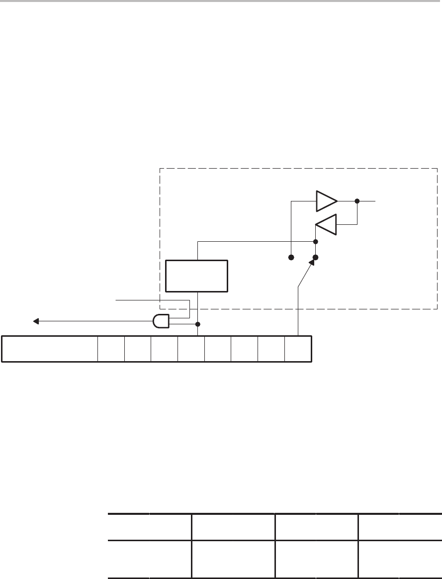
10.3.5 Using I/O Pins IO3, IO2, IO1, and IO0
Pins IO3, IO2, IO1, and IO0 can be individually configured as inputs or outputs
and can be used as handshake control for the asynchronous serial port or as
general-purpose I/O pins. They are software-controlled through the asynchro-
nous serial port control register (ASPCR) and the I/O status register (IOSR),
as shown in Figure 10–5.
Figure 10–5. Example of the Logic for Pins IO0–IO3
Level change
detect
CIO0bit=1 CIO0bit=0
General-purpose
I/O pin
IO0
DIO3 DIO2 DIO1 DIO0 IO3 IO2 IO1 IO0
Delta interrupt
I/O status register (IOSR)
DIM bit
The four LSBs of the ASPCR, bits CIO0–CIO3, are for configuring each pin as
an input or an output. For example, as shown in the figure, setting CIO0 to 1
configures IO0 as an output; setting CIO0 to 0 configures IO0 as an input. At
reset, CIO0–CIO3 are all cleared to 0, making all four of the the pins inputs.
Table 10–3 summarizes the configuration of the pins.
Table 10–3. Configuring Pins IO0–IO3 with ASPCR Bits CIO0–CIO3
CIO0
Bit
IO0
Pin
CIO1
Bit
IO1
Pin
CIO2
Bit
IO2
Pin
CIO3
Bit
IO3
Pin
0 Input 0 Input 0 Input 0 Input
1 Output 1 Output 1 Output 1 Output