
Calculator User Manual
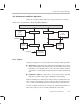
Table Of Contents
- Read This First
- Contents
- Figures
- Tables
- Examples
- Cautions
- Introduction
- Architectural Overview
- Central Processing Unit
- Memory and I/O Spaces
- Program Control
- Addressing Modes
- Assembly Language Instructions
- Instruction Set Summary
- How To Use the Instruction Descriptions
- Instruction Descriptions
- ABS
- ABS
- ADD
- ADD
- ADD
- ADD
- ADDC
- ADDC
- ADDS
- ADDS
- ADDT
- ADDT
- ADRK
- AND
- AND
- AND
- APAC
- APAC
- B
- BACC
- BANZ
- BANZ
- BCND
- BCND
- BIT
- BIT
- BITT
- BITT
- BLDD
- BLDD
- BLDD
- BLDD
- BLDD
- BLPD
- BLPD
- BLPD
- BLPD
- CALA
- CALL
- CC
- CC
- CLRC
- CLRC
- CMPL
- CMPR
- DMOV
- DMOV
- IDLE
- IN
- IN
- INTR
- LACC
- LACC
- LACC
- LACL
- LACL
- LACL
- LACT
- LACT
- LAR
- LAR
- LAR
- LDP
- LDP
- LPH
- LPH
- LST
- LST
- LST
- LST
- LT
- LT
- LTA
- LTA
- LTD
- LTD
- LTD
- LTP
- LTP
- LTS
- LTS
- MAC
- MAC
- MAC
- MAC
- MACD
- MACD
- MACD
- MACD
- MACD
- MAR
- MAR
- MPY
- MPY
- MPY
- MPYA
- MPYA
- MPYS
- MPYS
- MPYU
- MPYU
- NEG
- NEG
- NMI
- NOP
- NORM
- NORM
- NORM
- OR
- OR
- OR
- OUT
- OUT
- PAC
- POP
- POP
- POPD
- POPD
- PSHD
- PSHD
- PUSH
- RET
- RETC
- ROL
- ROR
- RPT
- RPT
- SACH
- SACH
- SACL
- SACL
- SAR
- SAR
- SBRK
- SETC
- SETC
- SFL
- SFR
- SFR
- SPAC
- SPH
- SPH
- SPL
- SPL
- SPLK
- SPLK
- SPM
- SQRA
- SQRA
- SQRS
- SQRS
- SST
- SST
- SUB
- SUB
- SUB
- SUB
- SUBB
- SUBB
- SUBC
- SUBC
- SUBS
- SUBS
- SUBT
- SUBT
- TBLR
- TBLR
- TBLR
- TBLW
- TBLW
- TBLW
- TRAP
- XOR
- XOR
- XOR
- ZALR
- ZALR
- On-Chip Peripherals
- Synchronous Serial Port
- Asynchronous Serial Port
- TMS320C209
- Register Summary
- TMS320C1x/C2x/C2xx/C5x Instruction Set Comparison
- Program Examples
- Submitting ROM Codes to TI
- Design Considerations for Using XDS510 Emulator
- E.1 Designing Your Target System’s Emulator Connector (14-Pin Header)
- E.2 Bus Protocol
- E.3 Emulator Cable Pod
- E.4 Emulator Cable Pod Signal Timing
- E.5 Emulation Timing Calculations
- E.6 Connections Between the Emulator and the Target System
- E.7 Physical Dimensions for the 14-Pin Emulator Connector
- E.8 Emulation Design Considerations
- Glossary
- Index

Controlling and Resetting the Port
10-12
Bit 7 DIO3 — Change detect bit for IO3. DIO3 indicates whether a change has
occurred on the IO3 pin. A change can be detected only when IO3 is config-
ured as an input by the CIO3 bit of the ASPCR (CIO3 = 0) and the serial port
is enabled by the URST bit of the ASPCR (URST = 1). Writing a 1 to DIO3
clears it to 0.
The detection of a change on the IO3 pin also generates an interrupt
(TXRXINT).
DIO3 = 0 No change is detected on IO3.
DIO3 = 1 A change is detected on IO3.
Bit 6 DIO2 — Change detect bit for IO2. DIO2 indicates whether a change has
occurred on the IO2 pin. A change can be detected only when IO2 is config-
ured as an input by the CIO2 bit of the ASPCR (CIO2 = 0) and the serial port
is enabled by the URST bit of the ASPCR (URST = 1). Writing a 1 to DIO2
clears it to 0.
The detection of a change on the IO2 pin also generates an interrupt
(TXRXINT).
DIO2 = 0 No change is detected on IO2.
DIO2 = 1 A change is detected on IO2.
Bit 5 DIO1 — Change detect bit for IO1. DIO1 indicates whether a change has
occurred on the IO1 pin. A change can be detected only when IO1 is config-
ured as an input by the CIO1 bit of the ASPCR (CIO1 = 0) and the serial port
is enabled by the URST bit of the ASPCR (URST = 1). Writing a 1 to DIO1
clears it to 0.
The detection of a change on the IO1 pin also generates an interrupt
(TXRXINT).
DIO1 = 0 No change is detected on IO1.
DIO1 = 1 A change is detected on IO1.
Bit 4 DIO0 — Change detect bit for IO0. DIO0 indicates whether a change has
occurred on the IO0 pin. A change can be detected only when IO0 is config-
ured as an input by the CIO0 bit of the ASPCR (CIO0 = 0) and the serial port
is enabled by the URST bit of the ASPCR (URST = 1). Writing a 1 to DIO0
clears it to 0.
The detection of a change on the IO0 pin also generates an interrupt
(TXRXINT).
DIO0 = 0 No change is detected on IO0.
DIO0 = 1 A change is detected on IO0.