
Calculator User Manual
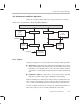
Table Of Contents
- Read This First
- Contents
- Figures
- Tables
- Examples
- Cautions
- Introduction
- Architectural Overview
- Central Processing Unit
- Memory and I/O Spaces
- Program Control
- Addressing Modes
- Assembly Language Instructions
- Instruction Set Summary
- How To Use the Instruction Descriptions
- Instruction Descriptions
- ABS
- ABS
- ADD
- ADD
- ADD
- ADD
- ADDC
- ADDC
- ADDS
- ADDS
- ADDT
- ADDT
- ADRK
- AND
- AND
- AND
- APAC
- APAC
- B
- BACC
- BANZ
- BANZ
- BCND
- BCND
- BIT
- BIT
- BITT
- BITT
- BLDD
- BLDD
- BLDD
- BLDD
- BLDD
- BLPD
- BLPD
- BLPD
- BLPD
- CALA
- CALL
- CC
- CC
- CLRC
- CLRC
- CMPL
- CMPR
- DMOV
- DMOV
- IDLE
- IN
- IN
- INTR
- LACC
- LACC
- LACC
- LACL
- LACL
- LACL
- LACT
- LACT
- LAR
- LAR
- LAR
- LDP
- LDP
- LPH
- LPH
- LST
- LST
- LST
- LST
- LT
- LT
- LTA
- LTA
- LTD
- LTD
- LTD
- LTP
- LTP
- LTS
- LTS
- MAC
- MAC
- MAC
- MAC
- MACD
- MACD
- MACD
- MACD
- MACD
- MAR
- MAR
- MPY
- MPY
- MPY
- MPYA
- MPYA
- MPYS
- MPYS
- MPYU
- MPYU
- NEG
- NEG
- NMI
- NOP
- NORM
- NORM
- NORM
- OR
- OR
- OR
- OUT
- OUT
- PAC
- POP
- POP
- POPD
- POPD
- PSHD
- PSHD
- PUSH
- RET
- RETC
- ROL
- ROR
- RPT
- RPT
- SACH
- SACH
- SACL
- SACL
- SAR
- SAR
- SBRK
- SETC
- SETC
- SFL
- SFR
- SFR
- SPAC
- SPH
- SPH
- SPL
- SPL
- SPLK
- SPLK
- SPM
- SQRA
- SQRA
- SQRS
- SQRS
- SST
- SST
- SUB
- SUB
- SUB
- SUB
- SUBB
- SUBB
- SUBC
- SUBC
- SUBS
- SUBS
- SUBT
- SUBT
- TBLR
- TBLR
- TBLR
- TBLW
- TBLW
- TBLW
- TRAP
- XOR
- XOR
- XOR
- ZALR
- ZALR
- On-Chip Peripherals
- Synchronous Serial Port
- Asynchronous Serial Port
- TMS320C209
- Register Summary
- TMS320C1x/C2x/C2xx/C5x Instruction Set Comparison
- Program Examples
- Submitting ROM Codes to TI
- Design Considerations for Using XDS510 Emulator
- E.1 Designing Your Target System’s Emulator Connector (14-Pin Header)
- E.2 Bus Protocol
- E.3 Emulator Cable Pod
- E.4 Emulator Cable Pod Signal Timing
- E.5 Emulation Timing Calculations
- E.6 Connections Between the Emulator and the Target System
- E.7 Physical Dimensions for the 14-Pin Emulator Connector
- E.8 Emulation Design Considerations
- Glossary
- Index

Controlling and Resetting the Port
10-11
Asynchronous Serial Port
Bit 11 THRE — Transmit register (ADTR) empty indicator. THRE is set to 1
when the contents of the transmit register (ADTR) are transferred to the
transmit shift register (AXSR). THRE is reset to 0 by the loading of the trans-
mit register with a new character. A device reset sets THRE to 1.
The emptying of the ADTR also generates an interrupt (TXRXINT).
THRE = 0 The transmit register is not empty. Port operation is normal.
THRE = 1 The transmit register is empty, indicating that it is ready to be
loaded with a new character.
Bit 10 FE — Framing error indicator. FE indicates whether a valid stop bit has
been detected during reception. Clear the FE bit to 0 by writing a 1 to it. It
is also cleared to 0 on reset.
A framing error also generates an interrupt (TXRXINT).
FE = 0 No framing error is detected. Port operation is normal.
FE = 1 The character received did not have a valid (logic 1) stop bit.
Bit 9 OE — Receive register (ADTR) overrun indicator. OE indicates whether
an unread character has been overwritten. Clear the OE bit to 0 by writing
a 1 to it. It is also cleared to 0 on reset.
The occurrence of overrun also generates an interrupt (TXRXINT).
OE = 0 No overrun error is detected. The port is operating normally.
OE = 1 The last character in the ADTR was not read before the next
character overwrote it.
Bit 8 DR — Data ready indicator for the receiver. This bit indicates whether a
new character has been received in the ADTR. This bit is automatically
cleared to zero when the receive register (ADTR) is read or when the device
is reset.
The reception of a new character into the ADTR also generates an interrupt
(TXRXINT).
DR = 0 The receive register (ADTR) is empty.
DR = 1 A character has been completely received and should be read
from the receive register (ADTR).