
Calculator User Manual
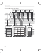
Table Of Contents
- Read This First
- Contents
- Figures
- Tables
- Examples
- Cautions
- Introduction
- Architectural Overview
- Central Processing Unit
- Memory and I/O Spaces
- Program Control
- Addressing Modes
- Assembly Language Instructions
- Instruction Set Summary
- How To Use the Instruction Descriptions
- Instruction Descriptions
- ABS
- ABS
- ADD
- ADD
- ADD
- ADD
- ADDC
- ADDC
- ADDS
- ADDS
- ADDT
- ADDT
- ADRK
- AND
- AND
- AND
- APAC
- APAC
- B
- BACC
- BANZ
- BANZ
- BCND
- BCND
- BIT
- BIT
- BITT
- BITT
- BLDD
- BLDD
- BLDD
- BLDD
- BLDD
- BLPD
- BLPD
- BLPD
- BLPD
- CALA
- CALL
- CC
- CC
- CLRC
- CLRC
- CMPL
- CMPR
- DMOV
- DMOV
- IDLE
- IN
- IN
- INTR
- LACC
- LACC
- LACC
- LACL
- LACL
- LACL
- LACT
- LACT
- LAR
- LAR
- LAR
- LDP
- LDP
- LPH
- LPH
- LST
- LST
- LST
- LST
- LT
- LT
- LTA
- LTA
- LTD
- LTD
- LTD
- LTP
- LTP
- LTS
- LTS
- MAC
- MAC
- MAC
- MAC
- MACD
- MACD
- MACD
- MACD
- MACD
- MAR
- MAR
- MPY
- MPY
- MPY
- MPYA
- MPYA
- MPYS
- MPYS
- MPYU
- MPYU
- NEG
- NEG
- NMI
- NOP
- NORM
- NORM
- NORM
- OR
- OR
- OR
- OUT
- OUT
- PAC
- POP
- POP
- POPD
- POPD
- PSHD
- PSHD
- PUSH
- RET
- RETC
- ROL
- ROR
- RPT
- RPT
- SACH
- SACH
- SACL
- SACL
- SAR
- SAR
- SBRK
- SETC
- SETC
- SFL
- SFR
- SFR
- SPAC
- SPH
- SPH
- SPL
- SPL
- SPLK
- SPLK
- SPM
- SQRA
- SQRA
- SQRS
- SQRS
- SST
- SST
- SUB
- SUB
- SUB
- SUB
- SUBB
- SUBB
- SUBC
- SUBC
- SUBS
- SUBS
- SUBT
- SUBT
- TBLR
- TBLR
- TBLR
- TBLW
- TBLW
- TBLW
- TRAP
- XOR
- XOR
- XOR
- ZALR
- ZALR
- On-Chip Peripherals
- Synchronous Serial Port
- Asynchronous Serial Port
- TMS320C209
- Register Summary
- TMS320C1x/C2x/C2xx/C5x Instruction Set Comparison
- Program Examples
- Submitting ROM Codes to TI
- Design Considerations for Using XDS510 Emulator
- E.1 Designing Your Target System’s Emulator Connector (14-Pin Header)
- E.2 Bus Protocol
- E.3 Emulator Cable Pod
- E.4 Emulator Cable Pod Signal Timing
- E.5 Emulation Timing Calculations
- E.6 Connections Between the Emulator and the Target System
- E.7 Physical Dimensions for the 14-Pin Emulator Connector
- E.8 Emulation Design Considerations
- Glossary
- Index

Memory and I/O Spaces
2-7
Architectural Overview
2.3 Memory and I/O Spaces
The ’C2xx memory is organized into four individually selectable spaces: pro-
gram, local data, global data, and I/O. These spaces form an address range
of 224K words.
All ’C2xx devices include 288 words of dual-access RAM (DARAM) for data
memory and 256 words of data/program DARAM. Depending on the device,
it may also have data/program single-access RAM (SARAM) and read-only
memory (ROM) or flash memory. Table 2–1 shows how much ROM, flash
memory, DARAM, and SARAM are available on the different ’C2xx devices.
Table 2–1. Program and Data Memory on the TMS320C2xx Devices
Memory Type ’C203 ’C204 ’F206 ’C209
ROM (words) – 4K – 4K
Flash memory (words) – – 32K –
DARAM (words) 544 544 544 544
Data (words)
288 288 288 288
Data/program (words)
256 256 256 256
SARAM (words)
– – 4K 4K
The ’C2xx also has CPU registers that are mapped in data memory space and
peripheral registers that are mapped in on-chip I/O space. The ’C2xx memory
types and features are introduced in the subsections following this paragraph.
For more details about the configuration and use of the ’C2xx memory and I/O
space, see Chapter 4,
Memory and I/O Space
.
2.3.1 Dual-Access On-Chip RAM
All ’C2xx devices have 544 words × 16-bits of on-chip DARAM, which can be
accessed twice per machine cycle. This memory is primarily intended to hold
data but, when needed, can also hold programs. It can be configured in one
of two ways:
All 544 words are configured as data memory.
288 words are configured as data memory, and 256 words are configured
as program memory.
Because DARAM can be accessed twice per cycle, it improves the speed of
the CPU. The CPU operates within a four-cycle pipeline. In this pipeline, the