
Calculator User Manual
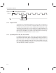
Table Of Contents
- Read This First
- Contents
- Figures
- Tables
- Examples
- Cautions
- Introduction
- Architectural Overview
- Central Processing Unit
- Memory and I/O Spaces
- Program Control
- Addressing Modes
- Assembly Language Instructions
- Instruction Set Summary
- How To Use the Instruction Descriptions
- Instruction Descriptions
- ABS
- ABS
- ADD
- ADD
- ADD
- ADD
- ADDC
- ADDC
- ADDS
- ADDS
- ADDT
- ADDT
- ADRK
- AND
- AND
- AND
- APAC
- APAC
- B
- BACC
- BANZ
- BANZ
- BCND
- BCND
- BIT
- BIT
- BITT
- BITT
- BLDD
- BLDD
- BLDD
- BLDD
- BLDD
- BLPD
- BLPD
- BLPD
- BLPD
- CALA
- CALL
- CC
- CC
- CLRC
- CLRC
- CMPL
- CMPR
- DMOV
- DMOV
- IDLE
- IN
- IN
- INTR
- LACC
- LACC
- LACC
- LACL
- LACL
- LACL
- LACT
- LACT
- LAR
- LAR
- LAR
- LDP
- LDP
- LPH
- LPH
- LST
- LST
- LST
- LST
- LT
- LT
- LTA
- LTA
- LTD
- LTD
- LTD
- LTP
- LTP
- LTS
- LTS
- MAC
- MAC
- MAC
- MAC
- MACD
- MACD
- MACD
- MACD
- MACD
- MAR
- MAR
- MPY
- MPY
- MPY
- MPYA
- MPYA
- MPYS
- MPYS
- MPYU
- MPYU
- NEG
- NEG
- NMI
- NOP
- NORM
- NORM
- NORM
- OR
- OR
- OR
- OUT
- OUT
- PAC
- POP
- POP
- POPD
- POPD
- PSHD
- PSHD
- PUSH
- RET
- RETC
- ROL
- ROR
- RPT
- RPT
- SACH
- SACH
- SACL
- SACL
- SAR
- SAR
- SBRK
- SETC
- SETC
- SFL
- SFR
- SFR
- SPAC
- SPH
- SPH
- SPL
- SPL
- SPLK
- SPLK
- SPM
- SQRA
- SQRA
- SQRS
- SQRS
- SST
- SST
- SUB
- SUB
- SUB
- SUB
- SUBB
- SUBB
- SUBC
- SUBC
- SUBS
- SUBS
- SUBT
- SUBT
- TBLR
- TBLR
- TBLR
- TBLW
- TBLW
- TBLW
- TRAP
- XOR
- XOR
- XOR
- ZALR
- ZALR
- On-Chip Peripherals
- Synchronous Serial Port
- Asynchronous Serial Port
- TMS320C209
- Register Summary
- TMS320C1x/C2x/C2xx/C5x Instruction Set Comparison
- Program Examples
- Submitting ROM Codes to TI
- Design Considerations for Using XDS510 Emulator
- E.1 Designing Your Target System’s Emulator Connector (14-Pin Header)
- E.2 Bus Protocol
- E.3 Emulator Cable Pod
- E.4 Emulator Cable Pod Signal Timing
- E.5 Emulation Timing Calculations
- E.6 Connections Between the Emulator and the Target System
- E.7 Physical Dimensions for the 14-Pin Emulator Connector
- E.8 Emulation Design Considerations
- Glossary
- Index
Timer
8-13
On-Chip Peripherals
8.4.4 Setting the Timer Interrupt Rate
When the divide-down value (TDDR) is 0, you can program the timer to gener-
ate an interrupt (TINT) every 2 to 65 536 cycles by programming the period
register (PRD) from 0 to 65 535 (FFFFh). When TDDR is nonzero (1 to 15),
the timer interrupt rate decreases.
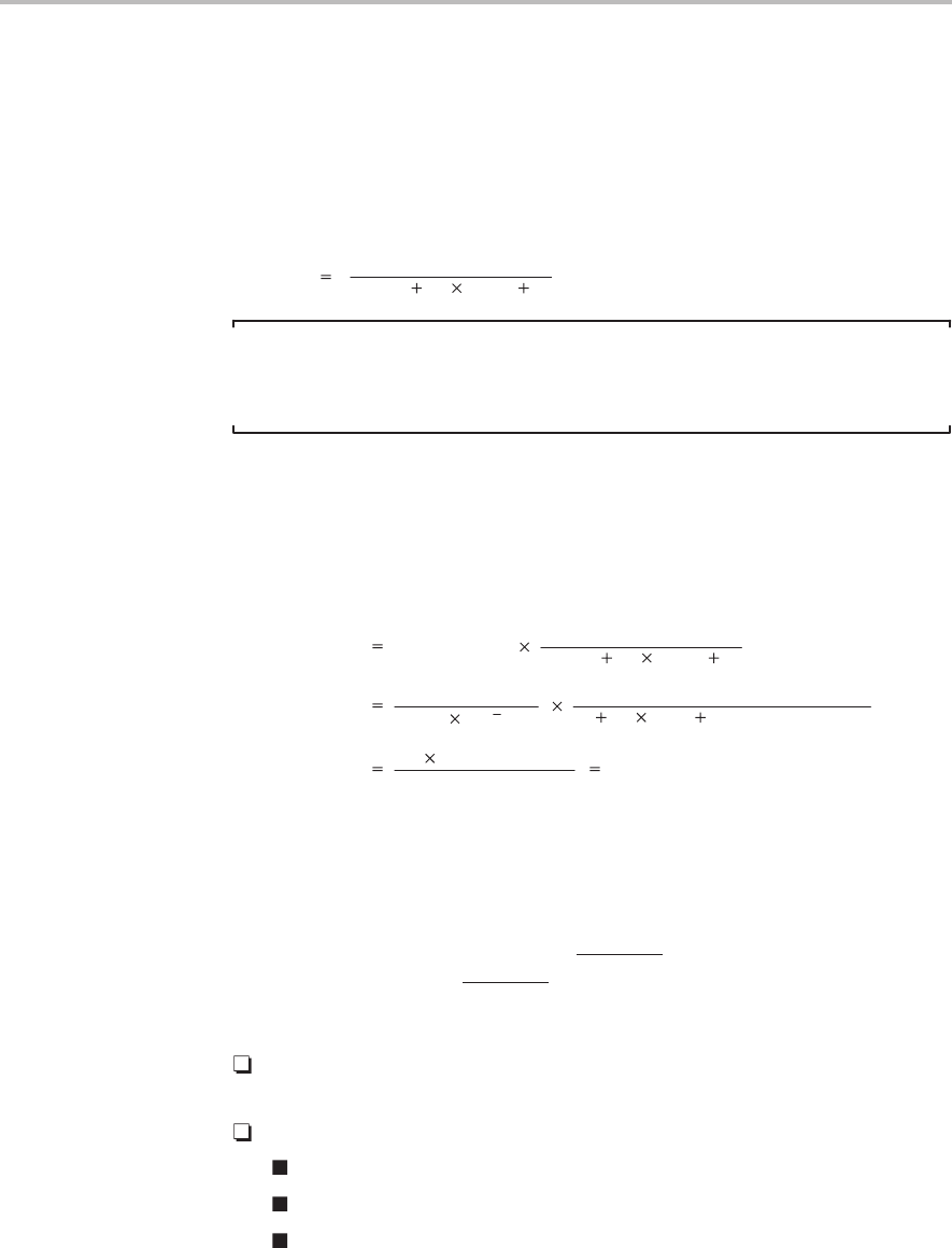
If TDDR, PRD, or both are nonzero, the timer interrupt rate is given by:
TINT rate
CLKOUT1 rate
(TDDR 1) (PRD 1)
Note:
When TDDR = PRD = 0, the timer interrupt rate defaults to
(CLKOUT1 rate)/2.
As an example of setting the timer interrupt rate, suppose the CLKOUT1 rate
is 10 MHz and you want to use the timer to generate a clock signal with a rate
of 10 kHz. You need to divide the CLKOUT1 rate by 1000. The TDDR is loaded
with 4, so that every 5 CLKOUT1 cycles, the TIM decrements by one. The PRD
is loaded with the starting count (199) for the TIM. These values are verified
with the TINT rate equation:
TINT rate CLKOUT1 rate
1
(TDDR 1) (PRD 1)
TINT rate
1 CLKOUT1 cycle
0.10 10
6
s
1 TINT cycle
(4 1) (199 1) CLKOUT1 cycles
TINT rate
10 10
3
TINT cycles
s
10 kHz
The PSC and the TIM would be loaded with the values from the TDDR and the
PRD, respectively. Then, one CLKOUT1 cycle after the TIM decrements to 0,
the timer would send an interrupt to the CPU.
8.4.5 The Timer at Hardware Reset
On a device reset, the CPU sends an SRESET signal to the peripheral circuits,
including the timer. The SRESET
signal has the following consequences on
the timer:
The registers TIM and PRD are loaded with their maximum values
(FFFFh).
All the bits of the TCR are cleared to zero with the following results:
The divide-down value is 0 (TDDR = 0 and PSC = 0).
The timer is started (TSS = 0).
The FREE and SOFT bits are both 0.