
Calculator User Manual
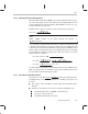
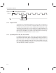
Table Of Contents
- Read This First
- Contents
- Figures
- Tables
- Examples
- Cautions
- Introduction
- Architectural Overview
- Central Processing Unit
- Memory and I/O Spaces
- Program Control
- Addressing Modes
- Assembly Language Instructions
- Instruction Set Summary
- How To Use the Instruction Descriptions
- Instruction Descriptions
- ABS
- ABS
- ADD
- ADD
- ADD
- ADD
- ADDC
- ADDC
- ADDS
- ADDS
- ADDT
- ADDT
- ADRK
- AND
- AND
- AND
- APAC
- APAC
- B
- BACC
- BANZ
- BANZ
- BCND
- BCND
- BIT
- BIT
- BITT
- BITT
- BLDD
- BLDD
- BLDD
- BLDD
- BLDD
- BLPD
- BLPD
- BLPD
- BLPD
- CALA
- CALL
- CC
- CC
- CLRC
- CLRC
- CMPL
- CMPR
- DMOV
- DMOV
- IDLE
- IN
- IN
- INTR
- LACC
- LACC
- LACC
- LACL
- LACL
- LACL
- LACT
- LACT
- LAR
- LAR
- LAR
- LDP
- LDP
- LPH
- LPH
- LST
- LST
- LST
- LST
- LT
- LT
- LTA
- LTA
- LTD
- LTD
- LTD
- LTP
- LTP
- LTS
- LTS
- MAC
- MAC
- MAC
- MAC
- MACD
- MACD
- MACD
- MACD
- MACD
- MAR
- MAR
- MPY
- MPY
- MPY
- MPYA
- MPYA
- MPYS
- MPYS
- MPYU
- MPYU
- NEG
- NEG
- NMI
- NOP
- NORM
- NORM
- NORM
- OR
- OR
- OR
- OUT
- OUT
- PAC
- POP
- POP
- POPD
- POPD
- PSHD
- PSHD
- PUSH
- RET
- RETC
- ROL
- ROR
- RPT
- RPT
- SACH
- SACH
- SACL
- SACL
- SAR
- SAR
- SBRK
- SETC
- SETC
- SFL
- SFR
- SFR
- SPAC
- SPH
- SPH
- SPL
- SPL
- SPLK
- SPLK
- SPM
- SQRA
- SQRA
- SQRS
- SQRS
- SST
- SST
- SUB
- SUB
- SUB
- SUB
- SUBB
- SUBB
- SUBC
- SUBC
- SUBS
- SUBS
- SUBT
- SUBT
- TBLR
- TBLR
- TBLR
- TBLW
- TBLW
- TBLW
- TRAP
- XOR
- XOR
- XOR
- ZALR
- ZALR
- On-Chip Peripherals
- Synchronous Serial Port
- Asynchronous Serial Port
- TMS320C209
- Register Summary
- TMS320C1x/C2x/C2xx/C5x Instruction Set Comparison
- Program Examples
- Submitting ROM Codes to TI
- Design Considerations for Using XDS510 Emulator
- E.1 Designing Your Target System’s Emulator Connector (14-Pin Header)
- E.2 Bus Protocol
- E.3 Emulator Cable Pod
- E.4 Emulator Cable Pod Signal Timing
- E.5 Emulation Timing Calculations
- E.6 Connections Between the Emulator and the Target System
- E.7 Physical Dimensions for the 14-Pin Emulator Connector
- E.8 Emulation Design Considerations
- Glossary
- Index
Timer
8-11
On-Chip Peripherals
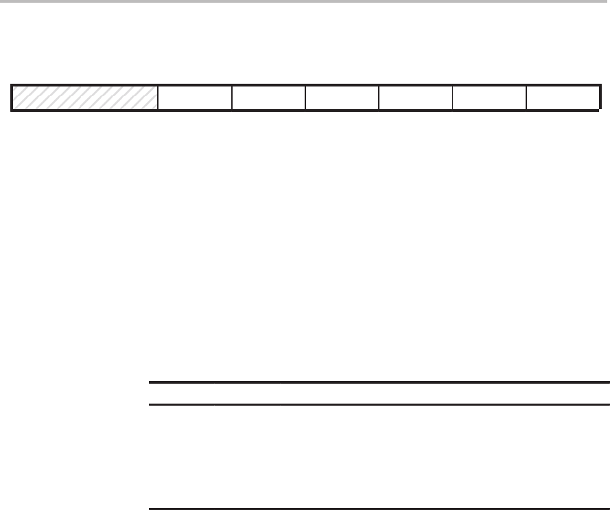
Figure 8–5. ’C2xx Timer Control Register (TCR) — I/O-Space Address FFF8h
15 12 11 10 965 430
Reserved FREE SOFT PSC TRB TSS TDDR
0 R/W–0 R/W–0 R/W–0 R/W–0 W–0 R/W–0
Note: 0 = Always read as zeros; R = Read access; W = Write access; value following dash (–) is value after reset.
Bits 15–12 Reserved. Bits 15–12 are reserved and are always read as 0s.
Bits 11–10 FREE, SOFT — These bits are special emulation bits that determine the
state of the timer when a breakpoint is encountered in the high-level lan-
guage debugger. If the FREE bit is set to 1, then, upon a software breakpoint,
the timer continues to run (that is, free runs). In this case, SOFT is a
don’t
care
. But if FREE is 0, then SOFT takes effect. In this case, if SOFT = 0, the
timer halts the next time the TIM decrements. If the SOFT bit is 1, then the
timer halts when the TIM has decremented to zero. Table 8–3 summarizes
the available run and emulation modes. The default (reset) setting is
FREE = 0 and SOFT = 0.
Table 8–3. ’C2xx Timer Run/Emulation Modes
FREE SOFT Timer Run/Emulation Mode
0 0 Stop after the next decrement of the TIM (hard stop)
0 1 Stop after the TIM decrements to 0 (soft stop)
1 0 Free run
1 1 Free run
Bits 9–6 PSC — Timer prescaler counter. These four bits hold the current prescale
count for the timer. For every CLKOUT1 cycle that the PSC value is greater
than 0, the PSC decrements by one. One CLKOUT1 cycle after the PSC
reaches 0, the PSC is loaded with the contents of the TDDR, and the timer
counter register (TIM) decrements by one. The PSC is also reloaded when-
ever the timer reload bit (TRB) is set by software. The PSC can be checked
by reading the TCR, but it cannot be set directly. It must get its value from
the timer divide-down register (TDDR). At reset, the PSC is set to 0.
Bit 5 TRB — Timer reload bit. When you write a 1 to TRB, the TIM is loaded with
the value in the PRD, and the PSC is loaded with the value in the timer divide-
down register (TDDR). The TRB bit is always read as zero.