
Calculator User Manual


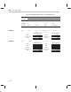
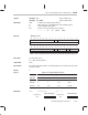

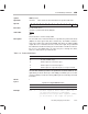
Table Of Contents
- Read This First
- Contents
- Figures
- Tables
- Examples
- Cautions
- Introduction
- Architectural Overview
- Central Processing Unit
- Memory and I/O Spaces
- Program Control
- Addressing Modes
- Assembly Language Instructions
- Instruction Set Summary
- How To Use the Instruction Descriptions
- Instruction Descriptions
- ABS
- ABS
- ADD
- ADD
- ADD
- ADD
- ADDC
- ADDC
- ADDS
- ADDS
- ADDT
- ADDT
- ADRK
- AND
- AND
- AND
- APAC
- APAC
- B
- BACC
- BANZ
- BANZ
- BCND
- BCND
- BIT
- BIT
- BITT
- BITT
- BLDD
- BLDD
- BLDD
- BLDD
- BLDD
- BLPD
- BLPD
- BLPD
- BLPD
- CALA
- CALL
- CC
- CC
- CLRC
- CLRC
- CMPL
- CMPR
- DMOV
- DMOV
- IDLE
- IN
- IN
- INTR
- LACC
- LACC
- LACC
- LACL
- LACL
- LACL
- LACT
- LACT
- LAR
- LAR
- LAR
- LDP
- LDP
- LPH
- LPH
- LST
- LST
- LST
- LST
- LT
- LT
- LTA
- LTA
- LTD
- LTD
- LTD
- LTP
- LTP
- LTS
- LTS
- MAC
- MAC
- MAC
- MAC
- MACD
- MACD
- MACD
- MACD
- MACD
- MAR
- MAR
- MPY
- MPY
- MPY
- MPYA
- MPYA
- MPYS
- MPYS
- MPYU
- MPYU
- NEG
- NEG
- NMI
- NOP
- NORM
- NORM
- NORM
- OR
- OR
- OR
- OUT
- OUT
- PAC
- POP
- POP
- POPD
- POPD
- PSHD
- PSHD
- PUSH
- RET
- RETC
- ROL
- ROR
- RPT
- RPT
- SACH
- SACH
- SACL
- SACL
- SAR
- SAR
- SBRK
- SETC
- SETC
- SFL
- SFR
- SFR
- SPAC
- SPH
- SPH
- SPL
- SPL
- SPLK
- SPLK
- SPM
- SQRA
- SQRA
- SQRS
- SQRS
- SST
- SST
- SUB
- SUB
- SUB
- SUB
- SUBB
- SUBB
- SUBC
- SUBC
- SUBS
- SUBS
- SUBT
- SUBT
- TBLR
- TBLR
- TBLR
- TBLW
- TBLW
- TBLW
- TRAP
- XOR
- XOR
- XOR
- ZALR
- ZALR
- On-Chip Peripherals
- Synchronous Serial Port
- Asynchronous Serial Port
- TMS320C209
- Register Summary
- TMS320C1x/C2x/C2xx/C5x Instruction Set Comparison
- Program Examples
- Submitting ROM Codes to TI
- Design Considerations for Using XDS510 Emulator
- E.1 Designing Your Target System’s Emulator Connector (14-Pin Header)
- E.2 Bus Protocol
- E.3 Emulator Cable Pod
- E.4 Emulator Cable Pod Signal Timing
- E.5 Emulation Timing Calculations
- E.6 Connections Between the Emulator and the Target System
- E.7 Physical Dimensions for the 14-Pin Emulator Connector
- E.8 Emulation Design Considerations
- Glossary
- Index

Set PREG Output Shift Mode
SPM
7-167
Assembly Language Instructions
Syntax SPM
constant
Operands constant: Value from 0 to 3 that determines the product shift mode
Opcode
constant00000011111101
0123456789101112131415
Execution Increment PC, then ...
constant → product shift mode (PM) bits
Status Bits
Affects
PM
This instruction is not affected by SXM.
Description The two LSBs of the instruction word are copied into the product shift mode
(PM) bits of status register ST1 (bits 1 and 0 of ST1). The PM bits control the
mode of the shifter at the output of the PREG. This shifter can shift the PREG
output either one or four bits to the left or six bits to the right. The possible PM
bit combinations and their meanings are shown in Table 7–8. When an instruc-
tion accesses the PREG value, the value first passes through the shifter,
where it is shifted by the specified amount.
Table 7–8. Product Shift Modes
PM Field Specified Product Shift
00 No shift of PREG output
01 PREG output to be left shifted 1 place
10 PREG output to be left shifted 4 places
11
PREG output to be right shifted 6 places and sign extended
The left shifts allow the product to be justified for fractional arithmetic. The
right-shift-by-six mode allows up to 128 multiply accumulate processes with-
out the possibility of overflow occurring. PM may also be loaded by an LST #1
instruction.
Words 1
Cycles for a Single SPM Instruction
ROM
DARAM SARAM External
1 1 1 1+p
Example SPM 3 ;Product register shift mode 3 (PM = 11)
;is selected causing all subsequent
;transfers from the product register (PREG)
;to be shifted to the right six places.
Cycles