
Calculator User Manual
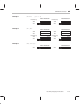
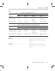
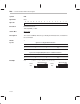

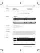
Table Of Contents
- Read This First
- Contents
- Figures
- Tables
- Examples
- Cautions
- Introduction
- Architectural Overview
- Central Processing Unit
- Memory and I/O Spaces
- Program Control
- Addressing Modes
- Assembly Language Instructions
- Instruction Set Summary
- How To Use the Instruction Descriptions
- Instruction Descriptions
- ABS
- ABS
- ADD
- ADD
- ADD
- ADD
- ADDC
- ADDC
- ADDS
- ADDS
- ADDT
- ADDT
- ADRK
- AND
- AND
- AND
- APAC
- APAC
- B
- BACC
- BANZ
- BANZ
- BCND
- BCND
- BIT
- BIT
- BITT
- BITT
- BLDD
- BLDD
- BLDD
- BLDD
- BLDD
- BLPD
- BLPD
- BLPD
- BLPD
- CALA
- CALL
- CC
- CC
- CLRC
- CLRC
- CMPL
- CMPR
- DMOV
- DMOV
- IDLE
- IN
- IN
- INTR
- LACC
- LACC
- LACC
- LACL
- LACL
- LACL
- LACT
- LACT
- LAR
- LAR
- LAR
- LDP
- LDP
- LPH
- LPH
- LST
- LST
- LST
- LST
- LT
- LT
- LTA
- LTA
- LTD
- LTD
- LTD
- LTP
- LTP
- LTS
- LTS
- MAC
- MAC
- MAC
- MAC
- MACD
- MACD
- MACD
- MACD
- MACD
- MAR
- MAR
- MPY
- MPY
- MPY
- MPYA
- MPYA
- MPYS
- MPYS
- MPYU
- MPYU
- NEG
- NEG
- NMI
- NOP
- NORM
- NORM
- NORM
- OR
- OR
- OR
- OUT
- OUT
- PAC
- POP
- POP
- POPD
- POPD
- PSHD
- PSHD
- PUSH
- RET
- RETC
- ROL
- ROR
- RPT
- RPT
- SACH
- SACH
- SACL
- SACL
- SAR
- SAR
- SBRK
- SETC
- SETC
- SFL
- SFR
- SFR
- SPAC
- SPH
- SPH
- SPL
- SPL
- SPLK
- SPLK
- SPM
- SQRA
- SQRA
- SQRS
- SQRS
- SST
- SST
- SUB
- SUB
- SUB
- SUB
- SUBB
- SUBB
- SUBC
- SUBC
- SUBS
- SUBS
- SUBT
- SUBT
- TBLR
- TBLR
- TBLR
- TBLW
- TBLW
- TBLW
- TRAP
- XOR
- XOR
- XOR
- ZALR
- ZALR
- On-Chip Peripherals
- Synchronous Serial Port
- Asynchronous Serial Port
- TMS320C209
- Register Summary
- TMS320C1x/C2x/C2xx/C5x Instruction Set Comparison
- Program Examples
- Submitting ROM Codes to TI
- Design Considerations for Using XDS510 Emulator
- E.1 Designing Your Target System’s Emulator Connector (14-Pin Header)
- E.2 Bus Protocol
- E.3 Emulator Cable Pod
- E.4 Emulator Cable Pod Signal Timing
- E.5 Emulation Timing Calculations
- E.6 Connections Between the Emulator and the Target System
- E.7 Physical Dimensions for the 14-Pin Emulator Connector
- E.8 Emulation Design Considerations
- Glossary
- Index

OR
OR With Accumulator
7-130
Status Bits None
This instruction is not affected by SXM.
Description An OR operation is performed on the contents of the accumulator and the con-
tents of the addressed data-memory location or a long-immediate value. The
long-immediate value may be shifted before the OR operation. The result re-
mains in the accumulator. All bit positions unoccupied by the data operand are
zero filled, regardless of the value of the SXM status bit. Thus, the high word
of the accumulator is unaffected by this instruction if direct or indirect address-
ing is used, or if immediate addressing is used with a shift of 0. Zeros are
shifted into the least significant bits of the operand if immediate addressing is
used with a nonzero shift count.
Words
Words Addressing mode
1 Direct or indirect
2 Long immediate
Cycles for a Single OR Instruction (Using Direct and Indirect Addressing)
Program
Operand ROM DARAM SARAM External
DARAM 1 1 1 1+p
SARAM 1 1 1, 2
†
1+p
External 1+d 1+d 1+d 2+d+p
†
If the operand and the code are in the same SARAM block
Cycles for a Repeat (RPT) Execution of an OR Instruction (Using Direct and
Indirect Addressing)
Program
Operand ROM DARAM SARAM External
DARAM n n n n+p
SARAM n n n, n+1
†
n+p
External n+nd n+nd n+nd n+1+p+nd
†
If the operand and the code are in the same SARAM block
Cycles for a Single OR Instruction (Using Long Immediate Addressing)
ROM DARAM SARAM External
2 2 2 2+2p
Cycles