
Calculator User Manual
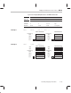
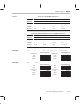

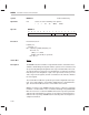
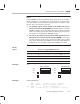
Table Of Contents
- Read This First
- Contents
- Figures
- Tables
- Examples
- Cautions
- Introduction
- Architectural Overview
- Central Processing Unit
- Memory and I/O Spaces
- Program Control
- Addressing Modes
- Assembly Language Instructions
- Instruction Set Summary
- How To Use the Instruction Descriptions
- Instruction Descriptions
- ABS
- ABS
- ADD
- ADD
- ADD
- ADD
- ADDC
- ADDC
- ADDS
- ADDS
- ADDT
- ADDT
- ADRK
- AND
- AND
- AND
- APAC
- APAC
- B
- BACC
- BANZ
- BANZ
- BCND
- BCND
- BIT
- BIT
- BITT
- BITT
- BLDD
- BLDD
- BLDD
- BLDD
- BLDD
- BLPD
- BLPD
- BLPD
- BLPD
- CALA
- CALL
- CC
- CC
- CLRC
- CLRC
- CMPL
- CMPR
- DMOV
- DMOV
- IDLE
- IN
- IN
- INTR
- LACC
- LACC
- LACC
- LACL
- LACL
- LACL
- LACT
- LACT
- LAR
- LAR
- LAR
- LDP
- LDP
- LPH
- LPH
- LST
- LST
- LST
- LST
- LT
- LT
- LTA
- LTA
- LTD
- LTD
- LTD
- LTP
- LTP
- LTS
- LTS
- MAC
- MAC
- MAC
- MAC
- MACD
- MACD
- MACD
- MACD
- MACD
- MAR
- MAR
- MPY
- MPY
- MPY
- MPYA
- MPYA
- MPYS
- MPYS
- MPYU
- MPYU
- NEG
- NEG
- NMI
- NOP
- NORM
- NORM
- NORM
- OR
- OR
- OR
- OUT
- OUT
- PAC
- POP
- POP
- POPD
- POPD
- PSHD
- PSHD
- PUSH
- RET
- RETC
- ROL
- ROR
- RPT
- RPT
- SACH
- SACH
- SACL
- SACL
- SAR
- SAR
- SBRK
- SETC
- SETC
- SFL
- SFR
- SFR
- SPAC
- SPH
- SPH
- SPL
- SPL
- SPLK
- SPLK
- SPM
- SQRA
- SQRA
- SQRS
- SQRS
- SST
- SST
- SUB
- SUB
- SUB
- SUB
- SUBB
- SUBB
- SUBC
- SUBC
- SUBS
- SUBS
- SUBT
- SUBT
- TBLR
- TBLR
- TBLR
- TBLW
- TBLW
- TBLW
- TRAP
- XOR
- XOR
- XOR
- ZALR
- ZALR
- On-Chip Peripherals
- Synchronous Serial Port
- Asynchronous Serial Port
- TMS320C209
- Register Summary
- TMS320C1x/C2x/C2xx/C5x Instruction Set Comparison
- Program Examples
- Submitting ROM Codes to TI
- Design Considerations for Using XDS510 Emulator
- E.1 Designing Your Target System’s Emulator Connector (14-Pin Header)
- E.2 Bus Protocol
- E.3 Emulator Cable Pod
- E.4 Emulator Cable Pod Signal Timing
- E.5 Emulation Timing Calculations
- E.6 Connections Between the Emulator and the Target System
- E.7 Physical Dimensions for the 14-Pin Emulator Connector
- E.8 Emulation Design Considerations
- Glossary
- Index

Normalize Contents of Accumulator
NORM
7-127
Assembly Language Instructions
Notes:
For the NORM instruction, the auxiliary register operations are executed dur-
ing the fourth phase of the pipeline, the execution phase. For other instruc-
tions, the auxiliary register operations take place in the second phase of the
pipeline, in the decode phase. Therefore:
1) The auxiliary register values should not be modified by the two
instruction words following NORM. If the auxiliary register used in the
NORM instruction is to be affected by either of the next two instruction
words, the auxiliary register value will be modified by the other instruc-
tions
before
it is modified by the NORM instruction.
2) The value in the auxiliary register pointer (ARP) should not be mo-
dified by the two instruction words following NORM. If either of the
next two instruction words specify a change in the ARP value, the ARP
value will be changed
before
NORM is executed; the ARP will not be
pointing at the correct auxiliary register when NORM is executed.
Words 1
Cycles for a Single NORM Instruction
ROM DARAM SARAM External
1 1 1 1+p
Cycles for a Repeat (RPT) Execution of a NORM Instruction
ROM
DARAM SARAM External
n n n n+p
Example 1 NORM *+
Before Instruction After Instruction
ARP 2 ARP 2
AR2 00h AR2 01h
ACC X 0FFFFF001h ACC X 0FFFE002h
CC
X0
TC TC
Example 2 31-Bit Normalization:
MAR *,AR1 ;Use AR1 to store the exponent.
LAR AR1,#0h ;Clear out exponent counter.
LOOP NORM *+ ;One bit is normalized.
BCND LOOP,NTC ;If TC = 0, magnitude not found yet.
Cycles