
Calculator User Manual
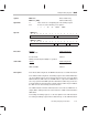
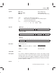
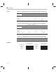
Table Of Contents
- Read This First
- Contents
- Figures
- Tables
- Examples
- Cautions
- Introduction
- Architectural Overview
- Central Processing Unit
- Memory and I/O Spaces
- Program Control
- Addressing Modes
- Assembly Language Instructions
- Instruction Set Summary
- How To Use the Instruction Descriptions
- Instruction Descriptions
- ABS
- ABS
- ADD
- ADD
- ADD
- ADD
- ADDC
- ADDC
- ADDS
- ADDS
- ADDT
- ADDT
- ADRK
- AND
- AND
- AND
- APAC
- APAC
- B
- BACC
- BANZ
- BANZ
- BCND
- BCND
- BIT
- BIT
- BITT
- BITT
- BLDD
- BLDD
- BLDD
- BLDD
- BLDD
- BLPD
- BLPD
- BLPD
- BLPD
- CALA
- CALL
- CC
- CC
- CLRC
- CLRC
- CMPL
- CMPR
- DMOV
- DMOV
- IDLE
- IN
- IN
- INTR
- LACC
- LACC
- LACC
- LACL
- LACL
- LACL
- LACT
- LACT
- LAR
- LAR
- LAR
- LDP
- LDP
- LPH
- LPH
- LST
- LST
- LST
- LST
- LT
- LT
- LTA
- LTA
- LTD
- LTD
- LTD
- LTP
- LTP
- LTS
- LTS
- MAC
- MAC
- MAC
- MAC
- MACD
- MACD
- MACD
- MACD
- MACD
- MAR
- MAR
- MPY
- MPY
- MPY
- MPYA
- MPYA
- MPYS
- MPYS
- MPYU
- MPYU
- NEG
- NEG
- NMI
- NOP
- NORM
- NORM
- NORM
- OR
- OR
- OR
- OUT
- OUT
- PAC
- POP
- POP
- POPD
- POPD
- PSHD
- PSHD
- PUSH
- RET
- RETC
- ROL
- ROR
- RPT
- RPT
- SACH
- SACH
- SACL
- SACL
- SAR
- SAR
- SBRK
- SETC
- SETC
- SFL
- SFR
- SFR
- SPAC
- SPH
- SPH
- SPL
- SPL
- SPLK
- SPLK
- SPM
- SQRA
- SQRA
- SQRS
- SQRS
- SST
- SST
- SUB
- SUB
- SUB
- SUB
- SUBB
- SUBB
- SUBC
- SUBC
- SUBS
- SUBS
- SUBT
- SUBT
- TBLR
- TBLR
- TBLR
- TBLW
- TBLW
- TBLW
- TRAP
- XOR
- XOR
- XOR
- ZALR
- ZALR
- On-Chip Peripherals
- Synchronous Serial Port
- Asynchronous Serial Port
- TMS320C209
- Register Summary
- TMS320C1x/C2x/C2xx/C5x Instruction Set Comparison
- Program Examples
- Submitting ROM Codes to TI
- Design Considerations for Using XDS510 Emulator
- E.1 Designing Your Target System’s Emulator Connector (14-Pin Header)
- E.2 Bus Protocol
- E.3 Emulator Cable Pod
- E.4 Emulator Cable Pod Signal Timing
- E.5 Emulation Timing Calculations
- E.6 Connections Between the Emulator and the Target System
- E.7 Physical Dimensions for the 14-Pin Emulator Connector
- E.8 Emulation Design Considerations
- Glossary
- Index
Modify Auxiliary Register
MAR
7-111
Assembly Language Instructions
Syntax MAR
dma
Direct addressing
MAR
ind
[, AR
n
] Indirect addressing
Operands n: Value from 0 to 7 designating the next auxiliary register
ind: Select one of the following seven options:
* *+ *– *0+ *0– *BR0+ *BR0–
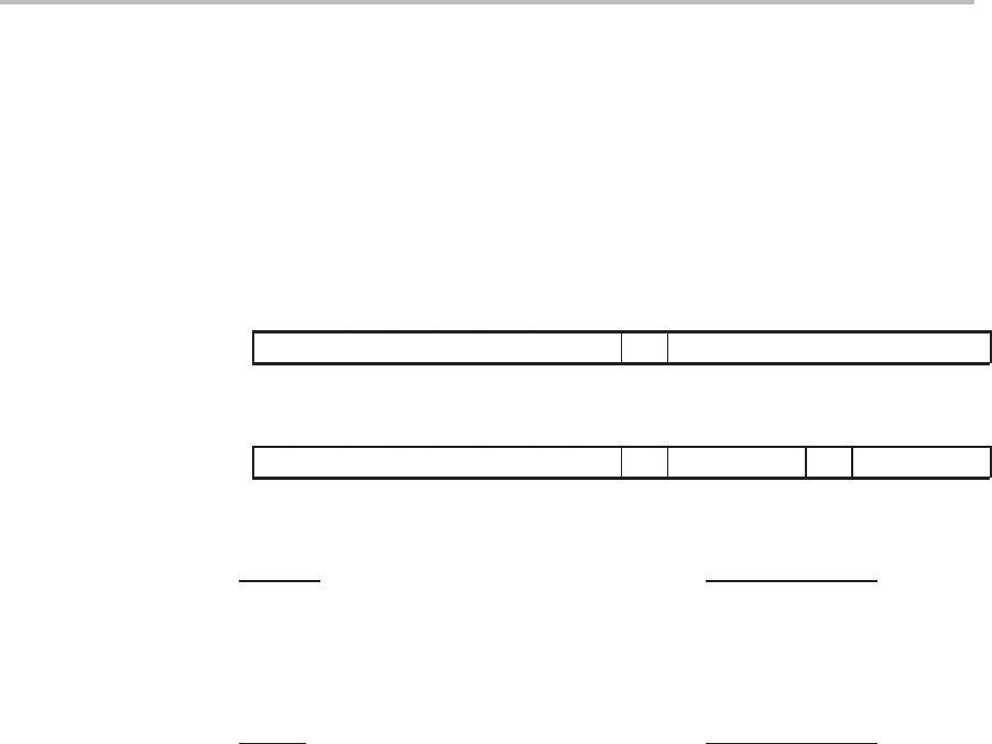
MAR
dma
1514131211109876543210
1
00010110 dma
MAR
ind
[, AR
n
]
1514131211109876543210
1
00010111 ARU N NAR
Note: ARU, N, and NAR are defined in Section 6.3,
Indirect Addressing Mode
(page 6-9).
Execution
Event(s) Addressing mode
Increment PC Direct
Increment PC Indirect
Modify (current AR) and (ARP) as specified
Status Bits
Affects Addressing mode
None Direct
ARP and ARB Indirect
Description In the direct addressing mode, the MAR instruction acts as a NOP instruction.
In the indirect addressing mode, an auxiliary register value and the ARP value
can be modified; however, the memory being referenced is not used. When
MAR modifies the ARP value, the old ARP value is copied to the ARB field of
ST1. Any operation that MAR performs with indirect addressing can also be
performed with any instruction that supports indirect addressing. In addition,
the ARP can also be loaded by an LST instruction.
The LARP instruction from the ’C25 instruction set is a subset of MAR. For ex-
ample, MAR *, AR4 performs the same function as LARP 4, which loads the
ARP with 4.
For loading an auxiliary register, see the description for the LAR instruction.
For storing an auxiliary register value to data memory, see the SAR instruction.
Opcode