
Calculator User Manual
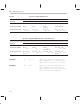

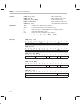
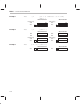
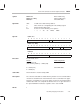
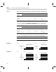
Table Of Contents
- Read This First
- Contents
- Figures
- Tables
- Examples
- Cautions
- Introduction
- Architectural Overview
- Central Processing Unit
- Memory and I/O Spaces
- Program Control
- Addressing Modes
- Assembly Language Instructions
- Instruction Set Summary
- How To Use the Instruction Descriptions
- Instruction Descriptions
- ABS
- ABS
- ADD
- ADD
- ADD
- ADD
- ADDC
- ADDC
- ADDS
- ADDS
- ADDT
- ADDT
- ADRK
- AND
- AND
- AND
- APAC
- APAC
- B
- BACC
- BANZ
- BANZ
- BCND
- BCND
- BIT
- BIT
- BITT
- BITT
- BLDD
- BLDD
- BLDD
- BLDD
- BLDD
- BLPD
- BLPD
- BLPD
- BLPD
- CALA
- CALL
- CC
- CC
- CLRC
- CLRC
- CMPL
- CMPR
- DMOV
- DMOV
- IDLE
- IN
- IN
- INTR
- LACC
- LACC
- LACC
- LACL
- LACL
- LACL
- LACT
- LACT
- LAR
- LAR
- LAR
- LDP
- LDP
- LPH
- LPH
- LST
- LST
- LST
- LST
- LT
- LT
- LTA
- LTA
- LTD
- LTD
- LTD
- LTP
- LTP
- LTS
- LTS
- MAC
- MAC
- MAC
- MAC
- MACD
- MACD
- MACD
- MACD
- MACD
- MAR
- MAR
- MPY
- MPY
- MPY
- MPYA
- MPYA
- MPYS
- MPYS
- MPYU
- MPYU
- NEG
- NEG
- NMI
- NOP
- NORM
- NORM
- NORM
- OR
- OR
- OR
- OUT
- OUT
- PAC
- POP
- POP
- POPD
- POPD
- PSHD
- PSHD
- PUSH
- RET
- RETC
- ROL
- ROR
- RPT
- RPT
- SACH
- SACH
- SACL
- SACL
- SAR
- SAR
- SBRK
- SETC
- SETC
- SFL
- SFR
- SFR
- SPAC
- SPH
- SPH
- SPL
- SPL
- SPLK
- SPLK
- SPM
- SQRA
- SQRA
- SQRS
- SQRS
- SST
- SST
- SUB
- SUB
- SUB
- SUB
- SUBB
- SUBB
- SUBC
- SUBC
- SUBS
- SUBS
- SUBT
- SUBT
- TBLR
- TBLR
- TBLR
- TBLW
- TBLW
- TBLW
- TRAP
- XOR
- XOR
- XOR
- ZALR
- ZALR
- On-Chip Peripherals
- Synchronous Serial Port
- Asynchronous Serial Port
- TMS320C209
- Register Summary
- TMS320C1x/C2x/C2xx/C5x Instruction Set Comparison
- Program Examples
- Submitting ROM Codes to TI
- Design Considerations for Using XDS510 Emulator
- E.1 Designing Your Target System’s Emulator Connector (14-Pin Header)
- E.2 Bus Protocol
- E.3 Emulator Cable Pod
- E.4 Emulator Cable Pod Signal Timing
- E.5 Emulation Timing Calculations
- E.6 Connections Between the Emulator and the Target System
- E.7 Physical Dimensions for the 14-Pin Emulator Connector
- E.8 Emulation Design Considerations
- Glossary
- Index

Software Interrupt
INTR
7-71
Assembly Language Instructions
Syntax INTR
K
Operands K: Value from 0 to 31 that indicates the interrupt vector location
to branch to
Opcode
0123456789101112131415
K11001111101
Execution (PC) + 1 → stack
corresponding
interrupt
vector location → PC
Status Bits
Affects
INTM
This instruction is not affected by INTM.
Description The processor has locations for 32 interrupt vectors; each location is repre-
sented by a value K from 0 to 31. The INTR instruction is a software interrupt
that transfers program control to the program-memory address specified by
K. The vector at that address then leads to the corresponding interrupt service
routine. Thus, the instruction allows any one of the interrupt service routines
to be executed from your software. For a list of interrupts and their correspond-
ing K values, see subsection 5.6.2,
Interrupt Table
, on page 5-16. During ex-
ecution of the instruction, the value PC + 1 (the return address) is pushed onto
the stack. Neither the INTM bit nor the interrupt masks affect the INTR instruc-
tion. An INTR for the external interrupts looks exactly like an external interrupt
(an interrupt acknowledge is generated, and maskable interrupts are globally
disabled by setting INTM = 1).
Words 1
Cycles for a Single INTR Instruction
ROM
DARAM SARAM External
4 4 4 4+3p
†
†
The processor performs speculative fetching by reading two additional instruction words. If the
PC discontinuity is taken, these two instruction words are discarded.
Example INTR 3 ;PC + 1 is pushed onto the stack.
;Then control is passed to program
;memory location 6h.
Cycles