
Calculator User Manual
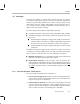
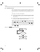
Table Of Contents
- Read This First
- Contents
- Figures
- Tables
- Examples
- Cautions
- Introduction
- Architectural Overview
- Central Processing Unit
- Memory and I/O Spaces
- Program Control
- Addressing Modes
- Assembly Language Instructions
- Instruction Set Summary
- How To Use the Instruction Descriptions
- Instruction Descriptions
- ABS
- ABS
- ADD
- ADD
- ADD
- ADD
- ADDC
- ADDC
- ADDS
- ADDS
- ADDT
- ADDT
- ADRK
- AND
- AND
- AND
- APAC
- APAC
- B
- BACC
- BANZ
- BANZ
- BCND
- BCND
- BIT
- BIT
- BITT
- BITT
- BLDD
- BLDD
- BLDD
- BLDD
- BLDD
- BLPD
- BLPD
- BLPD
- BLPD
- CALA
- CALL
- CC
- CC
- CLRC
- CLRC
- CMPL
- CMPR
- DMOV
- DMOV
- IDLE
- IN
- IN
- INTR
- LACC
- LACC
- LACC
- LACL
- LACL
- LACL
- LACT
- LACT
- LAR
- LAR
- LAR
- LDP
- LDP
- LPH
- LPH
- LST
- LST
- LST
- LST
- LT
- LT
- LTA
- LTA
- LTD
- LTD
- LTD
- LTP
- LTP
- LTS
- LTS
- MAC
- MAC
- MAC
- MAC
- MACD
- MACD
- MACD
- MACD
- MACD
- MAR
- MAR
- MPY
- MPY
- MPY
- MPYA
- MPYA
- MPYS
- MPYS
- MPYU
- MPYU
- NEG
- NEG
- NMI
- NOP
- NORM
- NORM
- NORM
- OR
- OR
- OR
- OUT
- OUT
- PAC
- POP
- POP
- POPD
- POPD
- PSHD
- PSHD
- PUSH
- RET
- RETC
- ROL
- ROR
- RPT
- RPT
- SACH
- SACH
- SACL
- SACL
- SAR
- SAR
- SBRK
- SETC
- SETC
- SFL
- SFR
- SFR
- SPAC
- SPH
- SPH
- SPL
- SPL
- SPLK
- SPLK
- SPM
- SQRA
- SQRA
- SQRS
- SQRS
- SST
- SST
- SUB
- SUB
- SUB
- SUB
- SUBB
- SUBB
- SUBC
- SUBC
- SUBS
- SUBS
- SUBT
- SUBT
- TBLR
- TBLR
- TBLR
- TBLW
- TBLW
- TBLW
- TRAP
- XOR
- XOR
- XOR
- ZALR
- ZALR
- On-Chip Peripherals
- Synchronous Serial Port
- Asynchronous Serial Port
- TMS320C209
- Register Summary
- TMS320C1x/C2x/C2xx/C5x Instruction Set Comparison
- Program Examples
- Submitting ROM Codes to TI
- Design Considerations for Using XDS510 Emulator
- E.1 Designing Your Target System’s Emulator Connector (14-Pin Header)
- E.2 Bus Protocol
- E.3 Emulator Cable Pod
- E.4 Emulator Cable Pod Signal Timing
- E.5 Emulation Timing Calculations
- E.6 Connections Between the Emulator and the Target System
- E.7 Physical Dimensions for the 14-Pin Emulator Connector
- E.8 Emulation Design Considerations
- Glossary
- Index
Interrupts
5-20
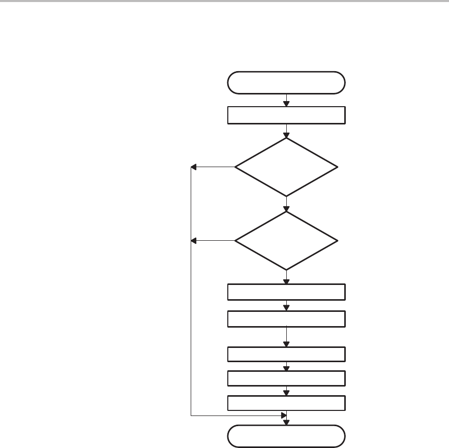
Figure 5–6 summarizes how maskable interrupts are handled by the CPU.
Figure 5–6. Maskable Interrupt Operation Flow Chart
Interrupt request sent to CPU
Corresponding IFR flag bit set
Interrupts enabled
(INTM bit = 0)
?
Interrupt
unmasked?
Interrupt acknowledged
Yes
Yes
No
No
INTM bit set to 1
PC saved on stack
Interrupt service routine run
Return instruction restores PC
Program continues
5.6.4 Interrupt Flag Register (IFR)
The 16-bit interrupt flag register (IFR), located at address 0006h in data
memory space, contains flag bits for all the maskable interrupts. When a mask-
able interrupt request reaches the CPU, the corresponding flag is set to 1 in
the IFR. This indicates that the interrupt is pending, or waiting for acknowl-
edgement.
Read the IFR to identify pending interrupts, and write to the IFR to clear pend-
ing interrupts. To clear an interrupt request (and set its IFR flag to 0), write a