
Calculator User Manual
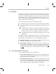
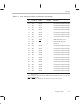
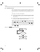
Table Of Contents
- Read This First
- Contents
- Figures
- Tables
- Examples
- Cautions
- Introduction
- Architectural Overview
- Central Processing Unit
- Memory and I/O Spaces
- Program Control
- Addressing Modes
- Assembly Language Instructions
- Instruction Set Summary
- How To Use the Instruction Descriptions
- Instruction Descriptions
- ABS
- ABS
- ADD
- ADD
- ADD
- ADD
- ADDC
- ADDC
- ADDS
- ADDS
- ADDT
- ADDT
- ADRK
- AND
- AND
- AND
- APAC
- APAC
- B
- BACC
- BANZ
- BANZ
- BCND
- BCND
- BIT
- BIT
- BITT
- BITT
- BLDD
- BLDD
- BLDD
- BLDD
- BLDD
- BLPD
- BLPD
- BLPD
- BLPD
- CALA
- CALL
- CC
- CC
- CLRC
- CLRC
- CMPL
- CMPR
- DMOV
- DMOV
- IDLE
- IN
- IN
- INTR
- LACC
- LACC
- LACC
- LACL
- LACL
- LACL
- LACT
- LACT
- LAR
- LAR
- LAR
- LDP
- LDP
- LPH
- LPH
- LST
- LST
- LST
- LST
- LT
- LT
- LTA
- LTA
- LTD
- LTD
- LTD
- LTP
- LTP
- LTS
- LTS
- MAC
- MAC
- MAC
- MAC
- MACD
- MACD
- MACD
- MACD
- MACD
- MAR
- MAR
- MPY
- MPY
- MPY
- MPYA
- MPYA
- MPYS
- MPYS
- MPYU
- MPYU
- NEG
- NEG
- NMI
- NOP
- NORM
- NORM
- NORM
- OR
- OR
- OR
- OUT
- OUT
- PAC
- POP
- POP
- POPD
- POPD
- PSHD
- PSHD
- PUSH
- RET
- RETC
- ROL
- ROR
- RPT
- RPT
- SACH
- SACH
- SACL
- SACL
- SAR
- SAR
- SBRK
- SETC
- SETC
- SFL
- SFR
- SFR
- SPAC
- SPH
- SPH
- SPL
- SPL
- SPLK
- SPLK
- SPM
- SQRA
- SQRA
- SQRS
- SQRS
- SST
- SST
- SUB
- SUB
- SUB
- SUB
- SUBB
- SUBB
- SUBC
- SUBC
- SUBS
- SUBS
- SUBT
- SUBT
- TBLR
- TBLR
- TBLR
- TBLW
- TBLW
- TBLW
- TRAP
- XOR
- XOR
- XOR
- ZALR
- ZALR
- On-Chip Peripherals
- Synchronous Serial Port
- Asynchronous Serial Port
- TMS320C209
- Register Summary
- TMS320C1x/C2x/C2xx/C5x Instruction Set Comparison
- Program Examples
- Submitting ROM Codes to TI
- Design Considerations for Using XDS510 Emulator
- E.1 Designing Your Target System’s Emulator Connector (14-Pin Header)
- E.2 Bus Protocol
- E.3 Emulator Cable Pod
- E.4 Emulator Cable Pod Signal Timing
- E.5 Emulation Timing Calculations
- E.6 Connections Between the Emulator and the Target System
- E.7 Physical Dimensions for the 14-Pin Emulator Connector
- E.8 Emulation Design Considerations
- Glossary
- Index

Interrupts
5-16
3) Execute the interrupt service routine. Once the interrupt is acknowl-
edged, the ’C2xx branches to its corresponding subroutine called an inter-
rupt service routine (ISR). The ’C2xx follows the branch instruction you
place at a predetermined address (the vector location) and executes the
ISR you have written.
5.6.2 Interrupt Table
For ’C2xx devices other than the ’C209, Table 5–5 lists the interrupts available
and shows their vector locations. In addition, it shows the priority of each of the
hardware interrupts. For the corresponding ’C209 table, see Section 11.3,
’C209 Interrupts
, on page 11-10.
Table 5–5. ’C2xx Interrupt Locations and Priorities
K
†
Vector
Location
Name Priority Function
0 0h RS 1 (highest)
Hardware reset (nonmaskable)
1 2h HOLD/INT1 4
User-maskable interrupt #1
2 4h INT2, INT3
‡
5
User-maskable interrupts #2
and #3
3 6h TINT 6
User-maskable timer interrupt
4 8h RINT 7 User-maskable synchronous
serial port receive interrupt
5 Ah XINT 8 User-maskable synchronous
serial port transmit interrupt
6 Ch TXRXINT 9 User-maskable asynchronous
serial port transmit/receive in-
terrupt
7 Eh 10 Reserved
8 10h INT8 – User-defined software interrupt
9 12h INT9 – User-defined software interrupt
Note: This table does not apply to the ’C209. For the ’C209 interrupt table, see Section 11.3
on page 11-10.
†
The K value is the operand used in an INTR instruction that branches to the corresponding
interrupt vector location.
‡
INT2
and INT3 have separate pins but are tied to the same vector location.