
Calculator User Manual
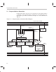
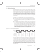
Table Of Contents
- Read This First
- Contents
- Figures
- Tables
- Examples
- Cautions
- Introduction
- Architectural Overview
- Central Processing Unit
- Memory and I/O Spaces
- Program Control
- Addressing Modes
- Assembly Language Instructions
- Instruction Set Summary
- How To Use the Instruction Descriptions
- Instruction Descriptions
- ABS
- ABS
- ADD
- ADD
- ADD
- ADD
- ADDC
- ADDC
- ADDS
- ADDS
- ADDT
- ADDT
- ADRK
- AND
- AND
- AND
- APAC
- APAC
- B
- BACC
- BANZ
- BANZ
- BCND
- BCND
- BIT
- BIT
- BITT
- BITT
- BLDD
- BLDD
- BLDD
- BLDD
- BLDD
- BLPD
- BLPD
- BLPD
- BLPD
- CALA
- CALL
- CC
- CC
- CLRC
- CLRC
- CMPL
- CMPR
- DMOV
- DMOV
- IDLE
- IN
- IN
- INTR
- LACC
- LACC
- LACC
- LACL
- LACL
- LACL
- LACT
- LACT
- LAR
- LAR
- LAR
- LDP
- LDP
- LPH
- LPH
- LST
- LST
- LST
- LST
- LT
- LT
- LTA
- LTA
- LTD
- LTD
- LTD
- LTP
- LTP
- LTS
- LTS
- MAC
- MAC
- MAC
- MAC
- MACD
- MACD
- MACD
- MACD
- MACD
- MAR
- MAR
- MPY
- MPY
- MPY
- MPYA
- MPYA
- MPYS
- MPYS
- MPYU
- MPYU
- NEG
- NEG
- NMI
- NOP
- NORM
- NORM
- NORM
- OR
- OR
- OR
- OUT
- OUT
- PAC
- POP
- POP
- POPD
- POPD
- PSHD
- PSHD
- PUSH
- RET
- RETC
- ROL
- ROR
- RPT
- RPT
- SACH
- SACH
- SACL
- SACL
- SAR
- SAR
- SBRK
- SETC
- SETC
- SFL
- SFR
- SFR
- SPAC
- SPH
- SPH
- SPL
- SPL
- SPLK
- SPLK
- SPM
- SQRA
- SQRA
- SQRS
- SQRS
- SST
- SST
- SUB
- SUB
- SUB
- SUB
- SUBB
- SUBB
- SUBC
- SUBC
- SUBS
- SUBS
- SUBT
- SUBT
- TBLR
- TBLR
- TBLR
- TBLW
- TBLW
- TBLW
- TRAP
- XOR
- XOR
- XOR
- ZALR
- ZALR
- On-Chip Peripherals
- Synchronous Serial Port
- Asynchronous Serial Port
- TMS320C209
- Register Summary
- TMS320C1x/C2x/C2xx/C5x Instruction Set Comparison
- Program Examples
- Submitting ROM Codes to TI
- Design Considerations for Using XDS510 Emulator
- E.1 Designing Your Target System’s Emulator Connector (14-Pin Header)
- E.2 Bus Protocol
- E.3 Emulator Cable Pod
- E.4 Emulator Cable Pod Signal Timing
- E.5 Emulation Timing Calculations
- E.6 Connections Between the Emulator and the Target System
- E.7 Physical Dimensions for the 14-Pin Emulator Connector
- E.8 Emulation Design Considerations
- Glossary
- Index
Program-Address Generation
5-3
Program Control
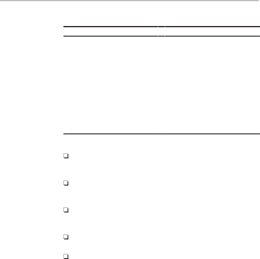
Table 5–1. Program-Address Generation Summary
Operation Program-Address Source
Sequential operation PC (contains program address +1)
Dummy cycle PAR (contains program address)
Return from subroutine Top of the stack (TOS)
Return from table move or block move Micro stack (MSTACK)
Branch or call to address specified in
instruction
Branch or call instruction by way of the
program read bus (PRDB)
Branch or call to address specified in
lower half of the accumulator
Low accumulator by way of the data
read bus (DRDB)
Branch to interrupt service routine Interrupt vector location by way of the
program read bus (PRDB)
The ’C2xx program-address generation logic uses the following hardware:
Program counter (PC). The ’C2xx has a 16-bit program counter (PC) that
addresses internal and external program memory when fetching instruc-
tions.
Program address register (PAR). The PAR drives the program address
bus (PAB). The PAB is a 16-bit bus that provides program addresses for
both reads and writes.
Stack. The program-address generation logic includes a 16-bit-wide, 8-
level hardware stack for storing up to eight return addresses. In addition,
you can use the stack for temporary storage.
Micro stack (MSTACK). Occasionally, the program-address generation
logic uses the 16-bit-wide, 1-level MSTACK to store one return address.
Repeat counter (RPTC). The 16-bit RPTC is used with the repeat (RPT)
instruction to determine how many times the instruction following RPT is
repeated.
5.1.1 Program Counter (PC)
The program-address generation logic uses the 16-bit program counter (PC)
to address internal and external program memory. The PC holds the address
of the next instruction to be executed. Through the program address bus
(PAB), an instruction is fetched from that address in program memory and
loaded into the instruction register. When the instruction register is loaded, the
PC holds the next address.