
Computer Hardware Algorithm Standard User's Guide
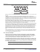
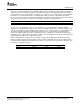

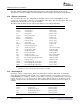
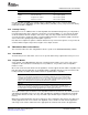
Table Of Contents
- Table of Contents
- Preface
- 1 Overview
- 2 General Programming Guidelines
- 3 Algorithm Component Model
- 3.1 Interfaces and Modules
- 3.1.1 External Identifiers
- 3.1.2 Naming Conventions
- 3.1.3 Module Initialization and Finalization
- 3.1.4 Module Instance Objects
- 3.1.5 Design-Time Object Creation
- 3.1.6 Run-Time Object Creation and Deletion
- 3.1.7 Module Configuration
- 3.1.8 Example Module
- 3.1.9 Multiple Interface Support
- 3.1.10 Interface Inheritance
- 3.1.11 Summary
- 3.2 Algorithms
- 3.3 Packaging
- 3.1 Interfaces and Modules
- 4 Algorithm Performance Characterization
- 5 DSP-Specific Guidelines
- 6 Use of the DMA Resource
- 6.1 Overview
- 6.2 Algorithm and Framework
- 6.3 Requirements for the Use of the DMA Resource
- 6.4 Logical Channel
- 6.5 Data Transfer Properties
- 6.6 Data Transfer Synchronization
- 6.7 Abstract Interface
- 6.8 Resource Characterization
- 6.9 Runtime APIs
- 6.10 Strong Ordering of DMA Transfer Requests
- 6.11 Submitting DMA Transfer Requests
- 6.12 Device Independent DMA Optimization Guideline
- 6.13 C6xxx Specific DMA Rules and Guidelines
- 6.14 C55x Specific DMA Rules and Guidelines
- 6.15 Inter-Algorithm Synchronization
- A Rules and Guidelines
- B Core Run-Time APIs
- C Bibliography
- D Glossary

www.ti.com
5.3.4 Register Conventions
5.3.5 Status Register
TMS320C6xxx Rules and Guidelines
In addition, no algorithm may ever directly manipulate the cache control registers. It is important to realize
that eXpressDSP-compliant algorithms may be placed in on-chip program memory by the system
developer. The rule above simply states that algorithms must not require placement in on-chip memory.
This section describes the rules and guidelines that apply to the use of the TMS320C6xxx on-chip
registers. As described above, there are several different register types. Note that any register that is not
described here must not be accessed by an algorithm.
The table below describes all of the registers that may be accessed by an algorithm.
Register Use Type
AMR=0 Address mode register Init (local)
A0-A9 General purpose Scratch (local)
A10-A14 General purpose Preserve (local)
A15 Frame pointer Preserve (local)
A16-A31 C64x general purpose Scratch (local)
B0-B9 General purpose Scratch (local)
B10-B13 General purpose Preserve (local)
B14 Data page pointer Preserve (local)
B15 Stack pointer Preserve (local)
B16-B31 C64x general purpose Scratch (local)
CSR Control and status register Preserve
ICR Interrupt clear register Not accessible (global)
IER Interrupt enable register Read-only (global)
IFR Interrupt flag register Read-only (global)
IRP
(1)
Interrupt return pointer Scratch (global)
ISR Interrupt set register Not accessible (global)
ISTP Interrupt service table pointer Read-only (global)
NRP Non-maskable Interrupt return pointer Read-only (global)
PCE1 Program counter Read-only (local)
FADCR C67xx floating point control register Preserve (local)
FAUCR C67xx floating point control register Preserve (local)
FMCR C67xx floating point control register Preserve (local)
(1)
IRP may be used as a scratch-pad register if interrupts are disabled.
The C6xxx contains a status register, CSR. This status register is further divided into several distinct
fields. Although each field is often thought of as a separate register, it is not possible to access these
fields individually. For example, in order to set one field it is necessary to set all fields in the same status
register. Therefore, it is necessary to treat the status registers with special care; if any field of a status
register is of type Preserve or Read-only, the entire register must be treated as a Preserve register, for
example.
CSR Field Use Type
SAT Saturation bit Scratch (local)
CPUID Identifies CPU Read-only (global)
RevId Identifies CPU revision Read-only (global)
GIE Global interrupt enable bit Read-only (global)
PGIE Previous GIE value. Read-only (global)
48 DSP-Specific Guidelines SPRU352G – June 2005 – Revised February 2007
Submit Documentation Feedback