
Datasheet
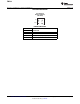
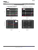

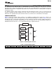

Table Of Contents
- FEATURES
- APPLICATIONS
- DESCRIPTION
- TYPICAL APPLICATION
- ABSOLUTE MAXIMUM RATINGS
- THERMAL INFORMATION
- ELECTRICAL CHARACTERISTICS
- PIN CONFIGURATION
- TYPICAL CHARACTERISTICS
- APPLICATION INFORMATION
- GENERAL DESCRIPTION
- COMMUNICATION PROTOCOL
- COMMAND REGISTER
- GLOBAL INITIALIZATION AND ADDRESS ASSIGNMENT SEQUENCE
- GLOBAL READ AND WRITE
- GLOBAL CLEAR INTERRUPT
- GLOBAL SOFTWARE RESET
- INDIVIDUAL READ AND WRITE
- TEMPERATURE REGISTER
- CONFIGURATION REGISTER
- TEMPERATURE LIMIT REGISTERS
- TIMEOUT FUNCTION
- NOISE
- SMAART WIRE INTERFACE TIMING SPECIFICATIONS
- Revision History

I/O
Control
Interface
RX
TX
Temperature
Register
Configuration
Register
T
LOW
Register
T
HIGH
Register
Command
Register
TMP104
www.ti.com
SBOS564A –NOVEMBER 2011– REVISED NOVEMBER 2011
The TMP104 has two dedicated pins for communication: TX and RX. Usually, these two pins are connected
internally and the signal on the RX propagates to the TX; that is, the TMP104 works in a transparent mode. The
TMP104 breaks this buffer configuration only when it must send data on the bus or during address assignment
and alert procedures.
The TMP104 supports unique address assignment and alert interrupt procedures. There are general-call read
and write commands that allow simultaneous reads or writes to all devices in the daisy-chain. The interface has
built-in time outs (typically 28 ms) that return the interface to a known state if communication is disrupted.
COMMAND REGISTER
Figure 6 shows the internal register structure of the TMP104. Communications between the registers are
transferred through the interface in LSB-first order. The 8-bit Command Register, as shown in Table 2, is used to
determine the type of instruction being addressed. These eight bits could either interpret a global instruction or
an individual instruction, which is determined by the value of P7. When P7 = 0, the command byte interprets an
individual instruction; when P7 = 1, the command byte interprets a global instruction.
Figure 6. Internal Register Structure
Table 2. Command Register Byte
P7 P6 P5 P4 P3 P2 P1 P0
GLB IN3/ID3 IN2/ID2 IN1/ID1 IN0/ID0 P1 P0 R/W
Copyright © 2011, Texas Instruments Incorporated Submit Documentation Feedback 7
Product Folder Link(s): TMP104