
Datasheet
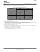

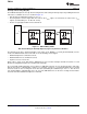


Table Of Contents
- FEATURES
- APPLICATIONS
- DESCRIPTION
- TYPICAL APPLICATION
- ABSOLUTE MAXIMUM RATINGS
- THERMAL INFORMATION
- ELECTRICAL CHARACTERISTICS
- PIN CONFIGURATION
- TYPICAL CHARACTERISTICS
- APPLICATION INFORMATION
- GENERAL DESCRIPTION
- COMMUNICATION PROTOCOL
- COMMAND REGISTER
- GLOBAL INITIALIZATION AND ADDRESS ASSIGNMENT SEQUENCE
- GLOBAL READ AND WRITE
- GLOBAL CLEAR INTERRUPT
- GLOBAL SOFTWARE RESET
- INDIVIDUAL READ AND WRITE
- TEMPERATURE REGISTER
- CONFIGURATION REGISTER
- TEMPERATURE LIMIT REGISTERS
- TIMEOUT FUNCTION
- NOISE
- SMAART WIRE INTERFACE TIMING SPECIFICATIONS
- Revision History
t
R
t
F
Baud
TYP
Jitter -
Jitter +
TMP104
SBOS564A –NOVEMBER 2011– REVISED NOVEMBER 2011
www.ti.com
SMAART WIRE INTERFACE TIMING SPECIFICATIONS
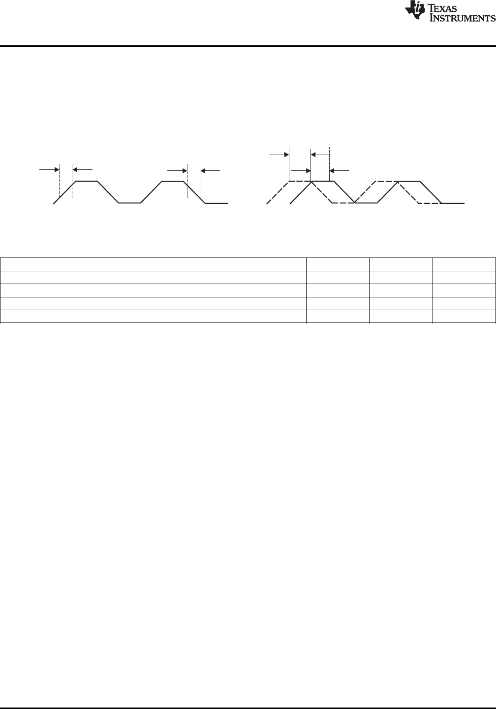
Figure 15 illustrates the key timing and jitter considerations for the SMAART wire interface. Table 10 contains the
timing specifications for ensured, reliable operation. During a transaction, the baud rate must remain within ±1%
of its initialization byte value; however, the baud rate can change from transaction to transaction. There is an
allowed delay between each byte transfer of less than 28 ms, which is the bus inactivity timeout check for the
TMP104 SMAART wire interface.
Figure 15. SMAART Wire Timing Diagram
Table 10. Timing Diagram Definitions
PARAMETER MIN MAX UNIT
Baud 4.8 k 114 k Bits/s
t
R
Clock/data rise time 0.5 %Baud
t
F
Clock/data fall time 0.5 %Baud
Jitter ±1 %Baud
16 Submit Documentation Feedback Copyright © 2011, Texas Instruments Incorporated
Product Folder Link(s): TMP104