
Datasheet


I C
2
MSP430F2112
TMP104D
TMP104C
TMP104B
TMP104A
10-Pin
Connector
JTAG Header
One-Wire UART
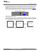
TMP104EVM Hardware Setup
www.ti.com
2.1 Theory of Operation for the TMP104 Hardware
Figure 3 shows the basic interactions that occur on the TMP104 Test Board. The board requires power
and I
2
C™ communication with the SM-USB-DIG. This configuration allows the TMP104EVM software to
communicate with the SM-USB-DIG and the TMP104 Test Board. In addition, test points allow for
application-specific connections to be used on the TMP104 Test Board.
Figure 3. TMP104EVM Board Block Diagram
2.2 Signal Definitions of H1 (10-Pin Male Connector Socket)
Table 3 shows the pinout for the 10-pin connector socket used to communicate between the TMP104EVM
and the SM-USB-DIG. It should be noted that the TMP104EVM uses only the necessary I
2
C
communication lines (pins 1 and 3) and the V
DUT
and GND (pins 6 and 8, respectively) to issue commands
to the TMP104.
Table 3. H1 Signal Definition for TMP104EVM
Pin on U1 Signal Description
1 I2C_SCL
I
2
C clock signal (SCL)
2 CTRL/MEAS4 GPIO: control output or measure input
3 I2C_SDA1
I
2
C data signal (SDA)
4 CTRL/MEAS5 GPIO: control output or measure input
5 SPI_DOUT1 SPI data output (MOSI)
Switchable DUT power supply: +3.3 V, +5 V,
6 V
DUT
Hi-Z (disconnected)
(1)
7 SPI_CLK SPI clock signal (SCLK)
8 GND Power return (GND)
9 SPI_CS1 SPI chip-select signal (CS)
10 SPI_DIN1 SPI data input (MISO)
(1)
When V
DUT
is Hi-Z, all digital I/O are Hi-Z as well.
4
TMP104EVM Evaluation Board and Software Tutorial SBOU118–October 2011
Submit Documentation Feedback
Copyright © 2011, Texas Instruments Incorporated