
Datasheet


VP_CLKOUTx
(PositiveEdge
Clocking)
VP_CLKOUTx
(NegativeEdge
Clocking)
VP_DOUTx
1
2
11 12
44
3
AM1808
www.ti.com
SPRS653E –FEBRUARY 2010–REVISED MARCH 2014
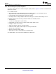
Table 6-117. Switching Characteristics Over Recommended Operating Conditions for Video Data Shown
With Respect to VP_CLKOUT2/3
(1)
(see Figure 6-75)
1.3V, 1.2V 1.1V 1.0V
NO. PARAMETER UNIT
MIN MAX MIN MAX MIN MAX
1 t
c(VKO)
Cycle time, VP_CLKOUT2/3 13.3 20 37 ns
2 t
w(VKOH)
Pulse duration, VP_CLKOUT2/3 high 0.4C 0.4C 0.4C ns
3 t
w(VKOL)
Pulse duration, VP_CLKOUT2/3 low 0.4C 0.4C 0.4C ns
4 t
t(VKO)
Transition time, VP_CLKOUT2/3 5 5 5 ns
Delay time,
11 t
d(VKOH-VPDOUTV)
8.5 12 17 ns
VP_CLKOUT2/3 high to VP_DOUTx valid
Delay time,
12 t
d(VCLKOH-VPDOUTIV)
1.5 1.5 1.5 ns
VP_CLKOUT2/3 high to VP_DOUTx invalid
(1) C = VP_CLKO2/3 period in ns.
Figure 6-75. VPIF Channels 2/3 Video Display Data Output Timing With Respect to VP_CLKOUT2/3
Copyright © 2010–2014, Texas Instruments Incorporated Peripheral Information and Electrical Specifications 227
Submit Documentation Feedback
Product Folder Links: AM1808