
Datasheet


Table Of Contents
- 1 Digital Media System-on-Chip (DMSoC)
- Table of Contents
- 2 Revision History
- 3 Device Overview
- 3.1 Device Characteristics
- 3.2 Device Compatibility
- 3.3 ARM Subsystem
- 3.3.1 ARM926EJ-S RISC CPU
- 3.3.2 CP15
- 3.3.3 MMU
- 3.3.4 Caches and Write Buffer
- 3.3.5 Tightly Coupled Memory (TCM)
- 3.3.6 Advanced High-Performance Bus (AHB)
- 3.3.7 Embedded Trace Macrocell (ETM) and Embedded Trace Buffer (ETB)
- 3.3.8 ARM Memory Mapping
- 3.3.9 Peripherals
- 3.3.10 PLL Controller (PLLC)
- 3.3.11 Power and Sleep Controller (PSC)
- 3.3.12 ARM Interrupt Controller (AINTC)
- 3.3.13 System Module
- 3.3.14 Power Management
- 3.4 DSP Subsystem
- 3.5 Memory Map Summary
- 3.6 Pin Assignments
- 3.7 Terminal Functions
- 3.8 Device Support
- 3.9 Documentation Support
- 3.10 Community Resources
- 4 Device Configurations
- 4.1 System Module Registers
- 4.2 Power Considerations
- 4.3 Clock Considerations
- 4.4 Boot Sequence
- 4.5 Configurations At Reset
- 4.6 Configurations After Reset
- 4.7 Multiplexed Pin Configurations
- 4.7.1 Pin Muxing Selection At Reset
- 4.7.2 Pin Muxing Selection After Reset
- 4.7.3 Pin Multiplexing Details
- 4.7.3.1 PCI, HPI, EMIFA, and ATA Pin Muxing
- 4.7.3.2 PWM Signal Muxing
- 4.7.3.3 TSIF0 Input Signal Muxing (Serial/Parallel)
- 4.7.3.4 TSIF0 Output Signal Muxing (Serial/Parallel)
- 4.7.3.5 TSIF1 Input Signal Muxing (Serial Only)
- 4.7.3.6 TSIF1 Output Signal Muxing (Serial Only)
- 4.7.3.7 CRGEN Signal Muxing
- 4.7.3.8 UART0 Pin Muxing
- 4.7.3.9 UART1 Pin Muxing
- 4.7.3.10 UART2 Pin Muxing
- 4.7.3.11 ARM/DSP Communications Interrupts
- 4.7.3.12 Emulation Control
- 4.8 Debugging Considerations
- 5 System Interconnect
- 6 Device Operating Conditions
- 7 Peripheral Information and Electrical Specifications
- 7.1 Parameter Information
- 7.2 Recommended Clock and Control Signal Transition Behavior
- 7.3 Power Supplies
- 7.4 External Clock Input From DEV_MXI/DEV_CLKIN and AUX_MXI/AUX_CLKIN Pins
- 7.5 Clock PLLs
- 7.6 Enhanced Direct Memory Access (EDMA3) Controller
- 7.7 Reset
- 7.8 Interrupts
- 7.9 External Memory Interface (EMIF)
- 7.10 DDR2 Memory Controller
- 7.10.1 DDR2 Memory Controller Electrical Data/Timing
- 7.10.2 DDR2 Interface
- 7.10.2.1 DDR2 Interface Schematic
- 7.10.2.2 Compatible JEDEC DDR2 Devices
- 7.10.2.3 PCB Stackup
- 7.10.2.4 Placement
- 7.10.2.5 DDR2 Keep Out Region
- 7.10.2.6 Bulk Bypass Capacitors
- 7.10.2.7 High-Speed Bypass Capacitors
- 7.10.2.8 Net Classes
- 7.10.2.9 DDR2 Signal Termination
- 7.10.2.10 VREF Routing
- 7.10.2.11 DDR2 CK and ADDR_CTRL Routing
- 7.11 Video Port Interface (VPIF)
- 7.12 Transport Stream Interface (TSIF)
- 7.13 Clock Recovery Generator (CRGEN)
- 7.14 Video Data Conversion Engine (VDCE)
- 7.15 Peripheral Component Interconnect (PCI)
- 7.16 Ethernet MAC (EMAC)
- 7.17 Management Data Input/Output (MDIO)
- 7.18 Host-Port Interface (HPI) Peripheral
- 7.19 USB 2.0 [see Note]
- 7.20 ATA Controller
- 7.21 VLYNQ
- 7.22 Multichannel Audio Serial Port (McASP0/1) Peripherals
- 7.23 Serial Peripheral Interface (SPI)
- 7.24 Universal Asynchronouse Receiver/Transmitter (UART)
- 7.25 Inter-Integrated Circuit (I2C)
- 7.26 Pulse Width Modulator (PWM)
- 7.27 Timers
- 7.28 General-Purpose Input/Output (GPIO)
- 7.29 IEEE 1149.1 JTAG
- 8 Mechanical Packaging and Orderable Information
TMS320DM6467T
www.ti.com
SPRS605C –JULY 2009–REVISED JUNE 2012
4.4.2.4 ARMBOOT Register
The ARM Boot Configuration (ARMBOOT) register is used to control the ARM926 boot. The ARMBOOT
value does not change as a result of a soft reset, instead the last value written is retained.
When ROM boot is selected (BTMODE[3:0] ≠ 0100), a jump to the internal TCM ROM (0x0000 8000) is
forced into the first fetched instruction word. The embedded ROM boot loader (RBL) code can then
perform certain configuration steps, read the BOOTCFG register to determine the desired boot method,
and branch to an appropriate secondary loader utility.
If EMIFA boot is selected (BTMODE[3:0] = 0100), a jump to the highest branch address (0x0200 0000) is
forced into the first fetched instruction word. This must be modified to address 0x4200 0000 in order to
map to the EMIFA. The ARM will then continue executing from external memory using the default EMIFA
timings until modified by software. Note: that either NOR Flash or ROM must be connected to the first
EMIFA chip select space (EM_CS2). The EMIFA does not support direct execution from NAND Flash.
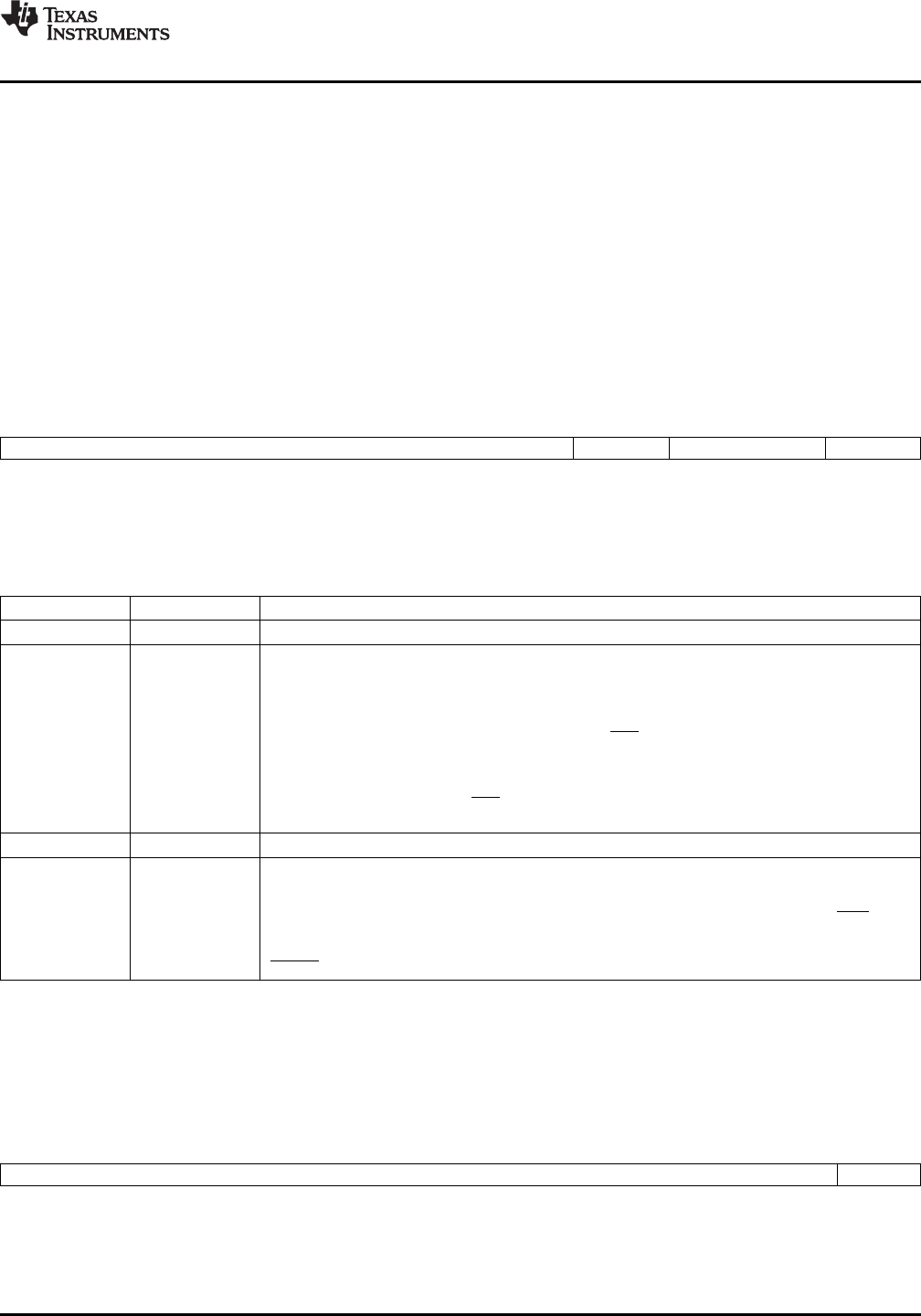
31 5 4 3 1 0
RESERVED ADDRMOD RESERVED TRAMBOOT
R-0000 0000 0000 0000 0000 0000 000 R/W-C R-000 R/W-0
LEGEND: R/W = Read/Write; R = Read only; C = Clear; -n = value after reset
Figure 4-9. ARMBOOT Register
Table 4-11. ARMBOOT Register Bit Descriptions
BIT NAME DESCRIPTION
31:5 RESERVED Reserved. Read returns "0".
IAHB Address Modification.
0 = No address modification.
1 = Address bit 30 is tied high to modify IAHB fetch address to point to EMIFA.
The default value for this bit is determined by the BOOTMODE configuration bits (BTMODE[3:0]). If
BTMODE[3:0] = 0100 [EMIFA direct boot (ROM/NOR)] , then ADDRMOD defaults to "1" so that
4 ADDRMOD instruction fetches from the ARM will point to EMIFA CS2 memory space. For all other
BTMODE[3:0] values, ADDRMOD defaults to "0" because ARM will boot from its TCM (ROM or
RAM).
The ADDRMOD value is ignored when TRAMBOOT is set (1) [address modification is disabled].
After branching into the EMIFA CS2 space, software should clear this bit as part of the reset routine
so that subsequent IAHB access addresses are not modified.
3:1 RESERVED Reserved. Read returns "0".
ARM TCM RAM Boot.
0 = Use BTMODE[3:0] selected boot mode
1 = Boot from ITCM RAM
0 TRAMBOOT This is a "sticky" bit that can be used to force the ARM926 to boot from ITCM RAM. On POR reset,
this bit will be initialized to "0" because TCM RAM is not initialized; otherwise, the bit retains the
value. After initializing ITCM RAM, software can set this bit so that subsequent Warm Reset
(RESET) or Soft Reset will boot from the ITCM.
4.4.2.5 ARMWAIT Register
The ARM Wait State Control (ARMWAIT) register is used to control ARM926 accesses to its TCM RAM.
At normal ARM operating frequency, a wait state must be inserted when accessing TCM RAM. When the
device is operated at low speeds, performance may be increased by removing the wait state. Note: TCM
ROM will always operate with a wait state enabled.
31 1 0
RESERVED RAMWAIT
R-0000 0000 0000 0000 0000 0000 0000 000 R/W-1
LEGEND: R/W = Read/Write; R = Read only; -n = value after reset
Figure 4-10. ARMWAIT Register
Copyright © 2009–2012, Texas Instruments Incorporated Device Configurations 97
Submit Documentation Feedback
Product Folder Link(s): TMS320DM6467T