
Datasheet


Table Of Contents
- 1 Digital Media System-on-Chip (DMSoC)
- Table of Contents
- 2 Revision History
- 3 Device Overview
- 3.1 Device Characteristics
- 3.2 Device Compatibility
- 3.3 ARM Subsystem
- 3.3.1 ARM926EJ-S RISC CPU
- 3.3.2 CP15
- 3.3.3 MMU
- 3.3.4 Caches and Write Buffer
- 3.3.5 Tightly Coupled Memory (TCM)
- 3.3.6 Advanced High-Performance Bus (AHB)
- 3.3.7 Embedded Trace Macrocell (ETM) and Embedded Trace Buffer (ETB)
- 3.3.8 ARM Memory Mapping
- 3.3.9 Peripherals
- 3.3.10 PLL Controller (PLLC)
- 3.3.11 Power and Sleep Controller (PSC)
- 3.3.12 ARM Interrupt Controller (AINTC)
- 3.3.13 System Module
- 3.3.14 Power Management
- 3.4 DSP Subsystem
- 3.5 Memory Map Summary
- 3.6 Pin Assignments
- 3.7 Terminal Functions
- 3.8 Device Support
- 3.9 Documentation Support
- 3.10 Community Resources
- 4 Device Configurations
- 4.1 System Module Registers
- 4.2 Power Considerations
- 4.3 Clock Considerations
- 4.4 Boot Sequence
- 4.5 Configurations At Reset
- 4.6 Configurations After Reset
- 4.7 Multiplexed Pin Configurations
- 4.7.1 Pin Muxing Selection At Reset
- 4.7.2 Pin Muxing Selection After Reset
- 4.7.3 Pin Multiplexing Details
- 4.7.3.1 PCI, HPI, EMIFA, and ATA Pin Muxing
- 4.7.3.2 PWM Signal Muxing
- 4.7.3.3 TSIF0 Input Signal Muxing (Serial/Parallel)
- 4.7.3.4 TSIF0 Output Signal Muxing (Serial/Parallel)
- 4.7.3.5 TSIF1 Input Signal Muxing (Serial Only)
- 4.7.3.6 TSIF1 Output Signal Muxing (Serial Only)
- 4.7.3.7 CRGEN Signal Muxing
- 4.7.3.8 UART0 Pin Muxing
- 4.7.3.9 UART1 Pin Muxing
- 4.7.3.10 UART2 Pin Muxing
- 4.7.3.11 ARM/DSP Communications Interrupts
- 4.7.3.12 Emulation Control
- 4.8 Debugging Considerations
- 5 System Interconnect
- 6 Device Operating Conditions
- 7 Peripheral Information and Electrical Specifications
- 7.1 Parameter Information
- 7.2 Recommended Clock and Control Signal Transition Behavior
- 7.3 Power Supplies
- 7.4 External Clock Input From DEV_MXI/DEV_CLKIN and AUX_MXI/AUX_CLKIN Pins
- 7.5 Clock PLLs
- 7.6 Enhanced Direct Memory Access (EDMA3) Controller
- 7.7 Reset
- 7.8 Interrupts
- 7.9 External Memory Interface (EMIF)
- 7.10 DDR2 Memory Controller
- 7.10.1 DDR2 Memory Controller Electrical Data/Timing
- 7.10.2 DDR2 Interface
- 7.10.2.1 DDR2 Interface Schematic
- 7.10.2.2 Compatible JEDEC DDR2 Devices
- 7.10.2.3 PCB Stackup
- 7.10.2.4 Placement
- 7.10.2.5 DDR2 Keep Out Region
- 7.10.2.6 Bulk Bypass Capacitors
- 7.10.2.7 High-Speed Bypass Capacitors
- 7.10.2.8 Net Classes
- 7.10.2.9 DDR2 Signal Termination
- 7.10.2.10 VREF Routing
- 7.10.2.11 DDR2 CK and ADDR_CTRL Routing
- 7.11 Video Port Interface (VPIF)
- 7.12 Transport Stream Interface (TSIF)
- 7.13 Clock Recovery Generator (CRGEN)
- 7.14 Video Data Conversion Engine (VDCE)
- 7.15 Peripheral Component Interconnect (PCI)
- 7.16 Ethernet MAC (EMAC)
- 7.17 Management Data Input/Output (MDIO)
- 7.18 Host-Port Interface (HPI) Peripheral
- 7.19 USB 2.0 [see Note]
- 7.20 ATA Controller
- 7.21 VLYNQ
- 7.22 Multichannel Audio Serial Port (McASP0/1) Peripherals
- 7.23 Serial Peripheral Interface (SPI)
- 7.24 Universal Asynchronouse Receiver/Transmitter (UART)
- 7.25 Inter-Integrated Circuit (I2C)
- 7.26 Pulse Width Modulator (PWM)
- 7.27 Timers
- 7.28 General-Purpose Input/Output (GPIO)
- 7.29 IEEE 1149.1 JTAG
- 8 Mechanical Packaging and Orderable Information
TMS320DM6467T
www.ti.com
SPRS605C –JULY 2009–REVISED JUNE 2012
4.3.3 Clock and Oscillator Control
The Clock and Oscillator Control (CLKCTL) register allows the user to disable the OSC pwrdwn and pwr
disable
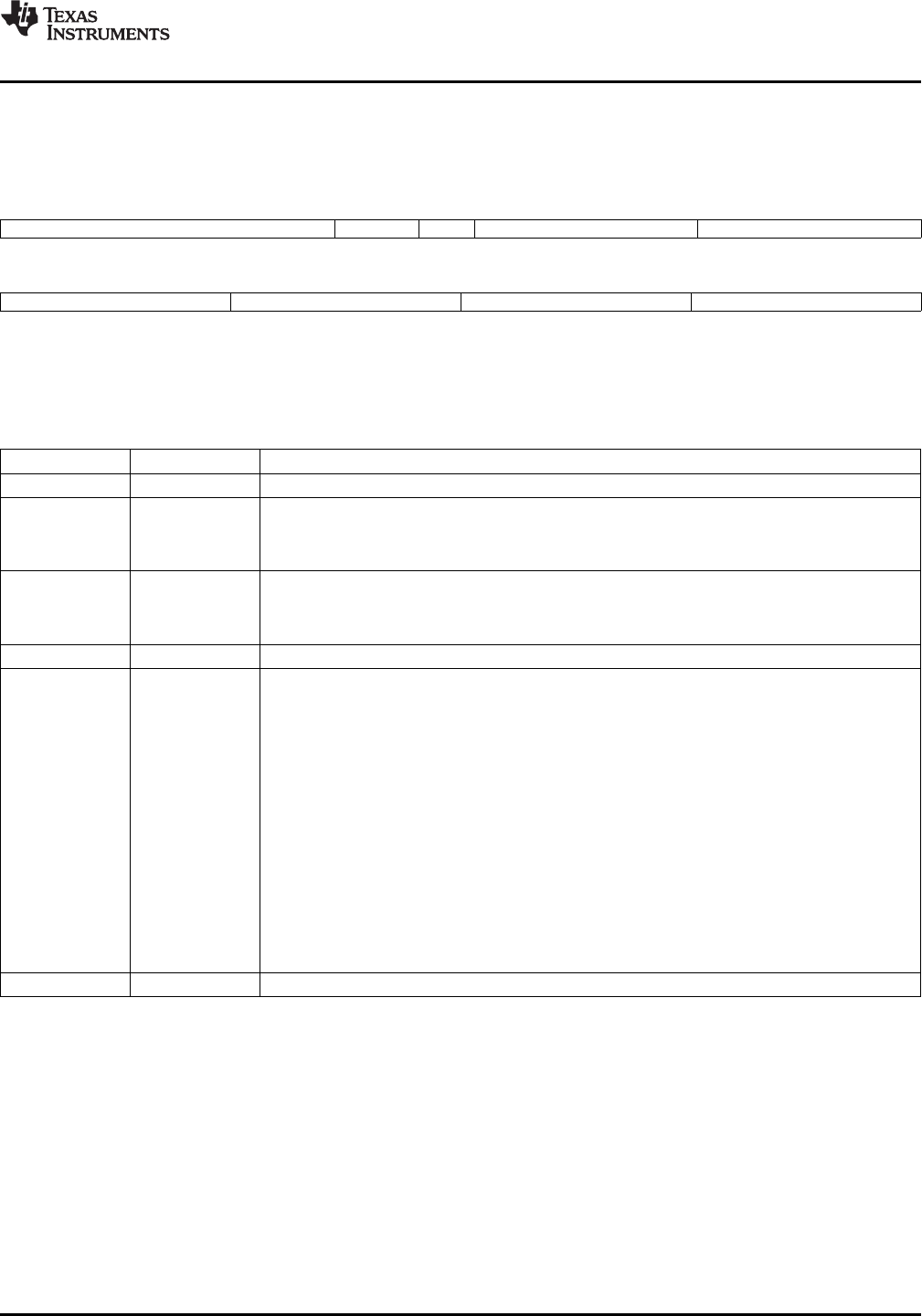
31 26 25 24 23 20 19 16
RESERVED OSCPWRDN OSCDIS RESERVED CLKOUT
R-0000 00 R/W-0 R/W-1 R-0000 R/W-1000
15 12 11 8 7 4 3 0
RESERVED AUD_CLK1 RESERVED AUD_CLK0
R-0000 R/W-0000 R-0000 R/W-0000
LEGEND: R/W = Read/Write; R = Read only; -n = value after reset
Figure 4-5. CLKCTL Register [0x01C4 005C]
Table 4-7. CLKCTL Register Bit Descriptions
BIT NAME DESCRIPTION
31:26 RESERVED Reserved. Read returns "0".
25 OSCPWRDN Auxiliary Oscillator Powerdown.
This bit controls the internal bias resistor conection.
0 = Internal bias resistor connected (normal operation)
1 = Internal bias resistor disconnected (external bias resistor required or clock input used)
24 OSCDIS Auxiliary Oscillator Disable.
This bit disables the oscillator.
0 = Oscillator enabled (normal operation).
1 = Oscillator disabled (clock input used or no Auxiliary clock required).
23:20 RESERVED Reserved. Read returns "0".
19:16 CLKOUT CLKOUT0 Source
(1)
This field selects the clock source for the CLKOUT0 output.
0000 = Disabled
0001 = PLL1 AUXCLK
0010 = Reserved
0011 = SYSCLK3
0100 = SYSCLK4
0101 = SYSCLK5
0110 = SYSCLK6
0111 = Reserved
1000 = SYSCLK8
1001 = SYSCLK9
1010 = AUX_MXI
1011 = Reserved
1100 = Reserved
1101 = Reserved
1110 = Reserved
1111 = Reserved
15:12 RESERVED Reserved. Read returns "0".
(1) The maximum frequency allowed for the CLKOUT0 pin is 148.5 MHz. Do not configure the CLKOUT bits to any SYSCLKx that is greater
than 148.5 MHz. For more details on the CLKOUT0 timings, see Table 7-14, Switching Characteristics Over Recommended Operating
Conditions for CLKOUT0.
Copyright © 2009–2012, Texas Instruments Incorporated Device Configurations 91
Submit Documentation Feedback
Product Folder Link(s): TMS320DM6467T