
Datasheet


Table Of Contents
- 1 Digital Media System-on-Chip (DMSoC)
- Table of Contents
- 2 Revision History
- 3 Device Overview
- 3.1 Device Characteristics
- 3.2 Device Compatibility
- 3.3 ARM Subsystem
- 3.3.1 ARM926EJ-S RISC CPU
- 3.3.2 CP15
- 3.3.3 MMU
- 3.3.4 Caches and Write Buffer
- 3.3.5 Tightly Coupled Memory (TCM)
- 3.3.6 Advanced High-Performance Bus (AHB)
- 3.3.7 Embedded Trace Macrocell (ETM) and Embedded Trace Buffer (ETB)
- 3.3.8 ARM Memory Mapping
- 3.3.9 Peripherals
- 3.3.10 PLL Controller (PLLC)
- 3.3.11 Power and Sleep Controller (PSC)
- 3.3.12 ARM Interrupt Controller (AINTC)
- 3.3.13 System Module
- 3.3.14 Power Management
- 3.4 DSP Subsystem
- 3.5 Memory Map Summary
- 3.6 Pin Assignments
- 3.7 Terminal Functions
- 3.8 Device Support
- 3.9 Documentation Support
- 3.10 Community Resources
- 4 Device Configurations
- 4.1 System Module Registers
- 4.2 Power Considerations
- 4.3 Clock Considerations
- 4.4 Boot Sequence
- 4.5 Configurations At Reset
- 4.6 Configurations After Reset
- 4.7 Multiplexed Pin Configurations
- 4.7.1 Pin Muxing Selection At Reset
- 4.7.2 Pin Muxing Selection After Reset
- 4.7.3 Pin Multiplexing Details
- 4.7.3.1 PCI, HPI, EMIFA, and ATA Pin Muxing
- 4.7.3.2 PWM Signal Muxing
- 4.7.3.3 TSIF0 Input Signal Muxing (Serial/Parallel)
- 4.7.3.4 TSIF0 Output Signal Muxing (Serial/Parallel)
- 4.7.3.5 TSIF1 Input Signal Muxing (Serial Only)
- 4.7.3.6 TSIF1 Output Signal Muxing (Serial Only)
- 4.7.3.7 CRGEN Signal Muxing
- 4.7.3.8 UART0 Pin Muxing
- 4.7.3.9 UART1 Pin Muxing
- 4.7.3.10 UART2 Pin Muxing
- 4.7.3.11 ARM/DSP Communications Interrupts
- 4.7.3.12 Emulation Control
- 4.8 Debugging Considerations
- 5 System Interconnect
- 6 Device Operating Conditions
- 7 Peripheral Information and Electrical Specifications
- 7.1 Parameter Information
- 7.2 Recommended Clock and Control Signal Transition Behavior
- 7.3 Power Supplies
- 7.4 External Clock Input From DEV_MXI/DEV_CLKIN and AUX_MXI/AUX_CLKIN Pins
- 7.5 Clock PLLs
- 7.6 Enhanced Direct Memory Access (EDMA3) Controller
- 7.7 Reset
- 7.8 Interrupts
- 7.9 External Memory Interface (EMIF)
- 7.10 DDR2 Memory Controller
- 7.10.1 DDR2 Memory Controller Electrical Data/Timing
- 7.10.2 DDR2 Interface
- 7.10.2.1 DDR2 Interface Schematic
- 7.10.2.2 Compatible JEDEC DDR2 Devices
- 7.10.2.3 PCB Stackup
- 7.10.2.4 Placement
- 7.10.2.5 DDR2 Keep Out Region
- 7.10.2.6 Bulk Bypass Capacitors
- 7.10.2.7 High-Speed Bypass Capacitors
- 7.10.2.8 Net Classes
- 7.10.2.9 DDR2 Signal Termination
- 7.10.2.10 VREF Routing
- 7.10.2.11 DDR2 CK and ADDR_CTRL Routing
- 7.11 Video Port Interface (VPIF)
- 7.12 Transport Stream Interface (TSIF)
- 7.13 Clock Recovery Generator (CRGEN)
- 7.14 Video Data Conversion Engine (VDCE)
- 7.15 Peripheral Component Interconnect (PCI)
- 7.16 Ethernet MAC (EMAC)
- 7.17 Management Data Input/Output (MDIO)
- 7.18 Host-Port Interface (HPI) Peripheral
- 7.19 USB 2.0 [see Note]
- 7.20 ATA Controller
- 7.21 VLYNQ
- 7.22 Multichannel Audio Serial Port (McASP0/1) Peripherals
- 7.23 Serial Peripheral Interface (SPI)
- 7.24 Universal Asynchronouse Receiver/Transmitter (UART)
- 7.25 Inter-Integrated Circuit (I2C)
- 7.26 Pulse Width Modulator (PWM)
- 7.27 Timers
- 7.28 General-Purpose Input/Output (GPIO)
- 7.29 IEEE 1149.1 JTAG
- 8 Mechanical Packaging and Orderable Information
TMS320DM6467T
www.ti.com
SPRS605C –JULY 2009–REVISED JUNE 2012
4.2 Power Considerations
The DM6467T provides several means of managing power consumption.
As described in the Section 7.3.4, DM6467T Power and Clock Domains, the DM6467T has one single
power domain—the “Always On” power domain. Within this power domain, the DM6467T utilizes local
clock gating via the Power and Sleep Controller (PSC) to achieve power savings. For more details on the
PSC, see Section 7.3.5, Power and Sleep Controller (PSC) and the TMS320DM646x DMSoC ARM
Subsystem Reference Guide (literature number SPRUEP9).
Some of the DM6467T peripherals support additional power saving features. For more details on power
saving features supported, see the peripheral-specific reference guides [listed/linked in the
TMS320DM646x DMSoC Peripherals Overview Reference Guide (literature number SPRUEQ0).
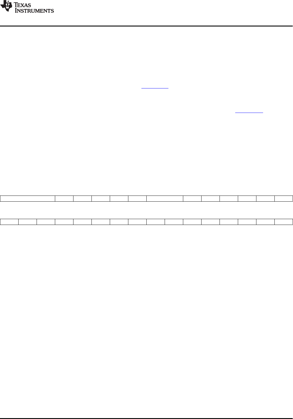
Most DM6467T 3.3-V I/Os can be powered-down to reduce power consumption. The VDD3P3V_PWDN
register in the System Module (see Figure 4-1 ) is used to selectively power down unused 3.3-V I/O pins.
Note: To save power, all other I/O buffers are powered down by default. Before using these pins, the user
must program the VDD3P3V_PWDN register to power up the corresponding I/O buffers.
For a list of multiplexed pins on the device and the pin mux group each pin belongs to, see Section 4.7.3,
Pin Multiplexing Details.
Note: The VDD3P3V_PWDN register only controls the power to the I/O buffers. The Power and Sleep
Controller (PSC) determines the clock/power state of the peripheral.
31 29 28 27 26 25 24 23 22 21 20 19 18 17 16
RESERVED USBV CLKOUT RSV SPI VLYNQ RESERVED GMII MII MCASP1 MCASP0 PCIHPI1 PCIHPI0
R-000 R/W-1 R/W-0 R-0 R/W-1 R/W-1 R-00 R/W-1 R/W-1 R/W-1 R/W-1 R/W-0 R/W-0
15 14 13 12 11 10 9 8 7 6 5 4 3 2 1 0
GPIO WDTIM TIM23 TIM01 PWM1 PWM0 UR2FC UR2DAT UR1FC UR1DAT UR0MDM UR0DF VPIF3 VPIF2 VPIF1 VPIF0
R/W-0 R/W-0 R/W-1 R/W-1 R/W-1 R/W-1 R/W-1 R/W-1 R/W-1 R/W-1 R/W-1 R/W-1 R/W-1 R/W-0 R/W-1 R/W-1
LEGEND: R/W = Read/Write; R = Read only; -n = value after reset
Figure 4-1. VDD3P3V_PWDN Register [0x01C4 0048]
Copyright © 2009–2012, Texas Instruments Incorporated Device Configurations 83
Submit Documentation Feedback
Product Folder Link(s): TMS320DM6467T