
Datasheet


Table Of Contents
- 1 Digital Media System-on-Chip (DMSoC)
- Table of Contents
- 2 Revision History
- 3 Device Overview
- 3.1 Device Characteristics
- 3.2 Device Compatibility
- 3.3 ARM Subsystem
- 3.3.1 ARM926EJ-S RISC CPU
- 3.3.2 CP15
- 3.3.3 MMU
- 3.3.4 Caches and Write Buffer
- 3.3.5 Tightly Coupled Memory (TCM)
- 3.3.6 Advanced High-Performance Bus (AHB)
- 3.3.7 Embedded Trace Macrocell (ETM) and Embedded Trace Buffer (ETB)
- 3.3.8 ARM Memory Mapping
- 3.3.9 Peripherals
- 3.3.10 PLL Controller (PLLC)
- 3.3.11 Power and Sleep Controller (PSC)
- 3.3.12 ARM Interrupt Controller (AINTC)
- 3.3.13 System Module
- 3.3.14 Power Management
- 3.4 DSP Subsystem
- 3.5 Memory Map Summary
- 3.6 Pin Assignments
- 3.7 Terminal Functions
- 3.8 Device Support
- 3.9 Documentation Support
- 3.10 Community Resources
- 4 Device Configurations
- 4.1 System Module Registers
- 4.2 Power Considerations
- 4.3 Clock Considerations
- 4.4 Boot Sequence
- 4.5 Configurations At Reset
- 4.6 Configurations After Reset
- 4.7 Multiplexed Pin Configurations
- 4.7.1 Pin Muxing Selection At Reset
- 4.7.2 Pin Muxing Selection After Reset
- 4.7.3 Pin Multiplexing Details
- 4.7.3.1 PCI, HPI, EMIFA, and ATA Pin Muxing
- 4.7.3.2 PWM Signal Muxing
- 4.7.3.3 TSIF0 Input Signal Muxing (Serial/Parallel)
- 4.7.3.4 TSIF0 Output Signal Muxing (Serial/Parallel)
- 4.7.3.5 TSIF1 Input Signal Muxing (Serial Only)
- 4.7.3.6 TSIF1 Output Signal Muxing (Serial Only)
- 4.7.3.7 CRGEN Signal Muxing
- 4.7.3.8 UART0 Pin Muxing
- 4.7.3.9 UART1 Pin Muxing
- 4.7.3.10 UART2 Pin Muxing
- 4.7.3.11 ARM/DSP Communications Interrupts
- 4.7.3.12 Emulation Control
- 4.8 Debugging Considerations
- 5 System Interconnect
- 6 Device Operating Conditions
- 7 Peripheral Information and Electrical Specifications
- 7.1 Parameter Information
- 7.2 Recommended Clock and Control Signal Transition Behavior
- 7.3 Power Supplies
- 7.4 External Clock Input From DEV_MXI/DEV_CLKIN and AUX_MXI/AUX_CLKIN Pins
- 7.5 Clock PLLs
- 7.6 Enhanced Direct Memory Access (EDMA3) Controller
- 7.7 Reset
- 7.8 Interrupts
- 7.9 External Memory Interface (EMIF)
- 7.10 DDR2 Memory Controller
- 7.10.1 DDR2 Memory Controller Electrical Data/Timing
- 7.10.2 DDR2 Interface
- 7.10.2.1 DDR2 Interface Schematic
- 7.10.2.2 Compatible JEDEC DDR2 Devices
- 7.10.2.3 PCB Stackup
- 7.10.2.4 Placement
- 7.10.2.5 DDR2 Keep Out Region
- 7.10.2.6 Bulk Bypass Capacitors
- 7.10.2.7 High-Speed Bypass Capacitors
- 7.10.2.8 Net Classes
- 7.10.2.9 DDR2 Signal Termination
- 7.10.2.10 VREF Routing
- 7.10.2.11 DDR2 CK and ADDR_CTRL Routing
- 7.11 Video Port Interface (VPIF)
- 7.12 Transport Stream Interface (TSIF)
- 7.13 Clock Recovery Generator (CRGEN)
- 7.14 Video Data Conversion Engine (VDCE)
- 7.15 Peripheral Component Interconnect (PCI)
- 7.16 Ethernet MAC (EMAC)
- 7.17 Management Data Input/Output (MDIO)
- 7.18 Host-Port Interface (HPI) Peripheral
- 7.19 USB 2.0 [see Note]
- 7.20 ATA Controller
- 7.21 VLYNQ
- 7.22 Multichannel Audio Serial Port (McASP0/1) Peripherals
- 7.23 Serial Peripheral Interface (SPI)
- 7.24 Universal Asynchronouse Receiver/Transmitter (UART)
- 7.25 Inter-Integrated Circuit (I2C)
- 7.26 Pulse Width Modulator (PWM)
- 7.27 Timers
- 7.28 General-Purpose Input/Output (GPIO)
- 7.29 IEEE 1149.1 JTAG
- 8 Mechanical Packaging and Orderable Information
TMS320DM6467T
www.ti.com
SPRS605C –JULY 2009–REVISED JUNE 2012
4 Device Configurations
4.1 System Module Registers
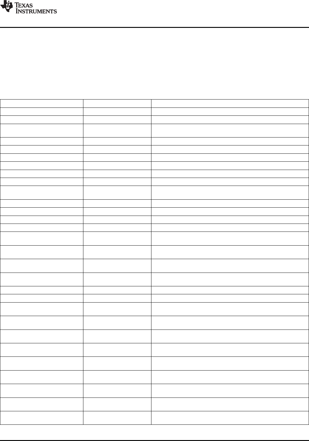
The system module includes status and control registers for configuration of the device.Brief descriptions
of the various registers are shown in Table 4-1. System Module registers required for device
configurations are discussed in the following sections.
Table 4-1. System Module Register Memory Map
HEX ADDRESS RANGE REGISTER ACRONYM DESCRIPTION
0x01C4 0000 PINMUX0 Pin Multiplexing Control 0 (see Section 4.7.2.1, PINMUX0 Register).
0x01C4 0004 PINMUX1 Pin Multiplexing Control 1 (see Section 4.7.2.2, PINMUX1 Register).
0x01C4 0008 DSPBOOTADDR DSP Boot Address. Decoded by bootloader software for host boots.
(See Section 4.4.2.1, DSPBOOTADDR Register.)
0x01C4 000C SUSPSRC Emulator Suspend Source (see Section 4.7.3.12, Emulation Control).
0x01C4 0010 BOOTSTAT Boot Status (see Section 4.4.2.2, BOOTSTAT Register).
0x01C4 0014 BOOTCFG Device Boot Configuration (see Section 4.4.2.3, BOOTCFG Register).
0x01C4 0018 – Reserved
0x01C4 001C - 0x01C4 0020 – Reserved
0x01C4 0024 ARMBOOT ARM926 Boot Control (see Section 4.4.2.4, ARMBOOT Register).
0x01C4 0028 JTAGID Device ID Number [see Section 7.29.1, JTAG ID (JTAGID) Register
Description(s)].
0x01C4 002C – Reserved
0x01C4 0030 HPICTL HPI Control (see Section 4.6.2.1, HPICTL Register).
0x01C4 0034 USBCTL USB Control (see Section 4.6.2.2, USBCTL Register).
0x01C4 0038 VIDCLKCTL Video Clock Control (see Section 4.3.2.1, Video Clock Control).
0x01C4 003C MSTPRI0 Bus Master Priority Control 0 (see Section 4.6.1, Switch Central
Resource (SCR) Bus Priorities).
0x01C4 0040 MSTPRI1 Bus Master Priority Control 1 (see Section 4.6.1, Switch Central
Resource (SCR) Bus Priorities).
0x01C4 0044 MSTPRI2 Bus Master Priority Control 2 (see Section 4.6.1, Switch Central
Resource (SCR) Bus Priorities).
0x01C4 0048 VDD3P3V_PWDN V
DD
3.3-V I/O Powerdown Control (see Section 4.2, Power
Considerations).
0x01C4 004C – Reserved
0x01C4 0050 TSIFCTL TSIF Control Register (see Section 4.3.2.2, TSIF Control).
0x01C4 0054 PWMCTL PWM Control (see Section 4.6.2.3, PWM (Trigger Source) Control
Register).
0x01C4 0058 EDMATCCFG EDMA TC Configuration (see Section 4.6.2.4, EDMATCCFG
Register).
0x01C4 005C CLKCTL Oscillator and Output Clock Control (see Section 4.3.3, Clock and
Oscillator Control).
0x01C4 0060 DSPINT ARM to DSP Interrupt Status (see Section 4.7.3.11, ARM/DSP
Communications Interrupts).
0x01C4 0064 DSPINTSET ARM to DSP Interrupt Set (see Section 4.7.3.11, ARM/DSP
Communications Interrupts).
0x01C4 0068 DSPINTCLR ARM to DSP Interrupt Clear (see Section 4.7.3.11, ARM/DSP
Communications Interrupts).
0x01C4 006C VSCLKDIS Video and TSIF Clock Disable (see Section 4.3.2.3, Video and TSIF
Clock Disable).
0x01C4 0070 ARMINT DSP to ARM Interrupt Status (see Section 4.7.3.11, ARM/DSP
Communications Interrupts).
0x01C4 0074 ARMINTSET DSP to ARM Interrupt Set (see Section 4.7.3.11, ARM/DSP
Communications Interrupts).
Copyright © 2009–2012, Texas Instruments Incorporated Device Configurations 81
Submit Documentation Feedback
Product Folder Link(s): TMS320DM6467T