
Datasheet


Table Of Contents
- 1 Digital Media System-on-Chip (DMSoC)
- Table of Contents
- 2 Revision History
- 3 Device Overview
- 3.1 Device Characteristics
- 3.2 Device Compatibility
- 3.3 ARM Subsystem
- 3.3.1 ARM926EJ-S RISC CPU
- 3.3.2 CP15
- 3.3.3 MMU
- 3.3.4 Caches and Write Buffer
- 3.3.5 Tightly Coupled Memory (TCM)
- 3.3.6 Advanced High-Performance Bus (AHB)
- 3.3.7 Embedded Trace Macrocell (ETM) and Embedded Trace Buffer (ETB)
- 3.3.8 ARM Memory Mapping
- 3.3.9 Peripherals
- 3.3.10 PLL Controller (PLLC)
- 3.3.11 Power and Sleep Controller (PSC)
- 3.3.12 ARM Interrupt Controller (AINTC)
- 3.3.13 System Module
- 3.3.14 Power Management
- 3.4 DSP Subsystem
- 3.5 Memory Map Summary
- 3.6 Pin Assignments
- 3.7 Terminal Functions
- 3.8 Device Support
- 3.9 Documentation Support
- 3.10 Community Resources
- 4 Device Configurations
- 4.1 System Module Registers
- 4.2 Power Considerations
- 4.3 Clock Considerations
- 4.4 Boot Sequence
- 4.5 Configurations At Reset
- 4.6 Configurations After Reset
- 4.7 Multiplexed Pin Configurations
- 4.7.1 Pin Muxing Selection At Reset
- 4.7.2 Pin Muxing Selection After Reset
- 4.7.3 Pin Multiplexing Details
- 4.7.3.1 PCI, HPI, EMIFA, and ATA Pin Muxing
- 4.7.3.2 PWM Signal Muxing
- 4.7.3.3 TSIF0 Input Signal Muxing (Serial/Parallel)
- 4.7.3.4 TSIF0 Output Signal Muxing (Serial/Parallel)
- 4.7.3.5 TSIF1 Input Signal Muxing (Serial Only)
- 4.7.3.6 TSIF1 Output Signal Muxing (Serial Only)
- 4.7.3.7 CRGEN Signal Muxing
- 4.7.3.8 UART0 Pin Muxing
- 4.7.3.9 UART1 Pin Muxing
- 4.7.3.10 UART2 Pin Muxing
- 4.7.3.11 ARM/DSP Communications Interrupts
- 4.7.3.12 Emulation Control
- 4.8 Debugging Considerations
- 5 System Interconnect
- 6 Device Operating Conditions
- 7 Peripheral Information and Electrical Specifications
- 7.1 Parameter Information
- 7.2 Recommended Clock and Control Signal Transition Behavior
- 7.3 Power Supplies
- 7.4 External Clock Input From DEV_MXI/DEV_CLKIN and AUX_MXI/AUX_CLKIN Pins
- 7.5 Clock PLLs
- 7.6 Enhanced Direct Memory Access (EDMA3) Controller
- 7.7 Reset
- 7.8 Interrupts
- 7.9 External Memory Interface (EMIF)
- 7.10 DDR2 Memory Controller
- 7.10.1 DDR2 Memory Controller Electrical Data/Timing
- 7.10.2 DDR2 Interface
- 7.10.2.1 DDR2 Interface Schematic
- 7.10.2.2 Compatible JEDEC DDR2 Devices
- 7.10.2.3 PCB Stackup
- 7.10.2.4 Placement
- 7.10.2.5 DDR2 Keep Out Region
- 7.10.2.6 Bulk Bypass Capacitors
- 7.10.2.7 High-Speed Bypass Capacitors
- 7.10.2.8 Net Classes
- 7.10.2.9 DDR2 Signal Termination
- 7.10.2.10 VREF Routing
- 7.10.2.11 DDR2 CK and ADDR_CTRL Routing
- 7.11 Video Port Interface (VPIF)
- 7.12 Transport Stream Interface (TSIF)
- 7.13 Clock Recovery Generator (CRGEN)
- 7.14 Video Data Conversion Engine (VDCE)
- 7.15 Peripheral Component Interconnect (PCI)
- 7.16 Ethernet MAC (EMAC)
- 7.17 Management Data Input/Output (MDIO)
- 7.18 Host-Port Interface (HPI) Peripheral
- 7.19 USB 2.0 [see Note]
- 7.20 ATA Controller
- 7.21 VLYNQ
- 7.22 Multichannel Audio Serial Port (McASP0/1) Peripherals
- 7.23 Serial Peripheral Interface (SPI)
- 7.24 Universal Asynchronouse Receiver/Transmitter (UART)
- 7.25 Inter-Integrated Circuit (I2C)
- 7.26 Pulse Width Modulator (PWM)
- 7.27 Timers
- 7.28 General-Purpose Input/Output (GPIO)
- 7.29 IEEE 1149.1 JTAG
- 8 Mechanical Packaging and Orderable Information
TMS320DM6467T
www.ti.com
SPRS605C –JULY 2009–REVISED JUNE 2012
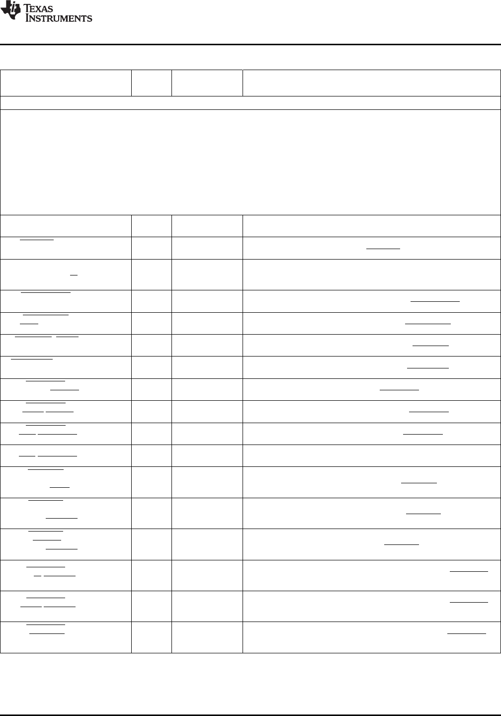
Table 3-11. Peripheral Component Interconnect (PCI) Terminal Functions
SIGNAL
TYPE
(1)
OTHER
(2) (3)
DESCRIPTION
NAME NO.
PCI
Notes: When PCI boot mode is not used, for proper device operation out of reset PCIEN must be "0".
The PCI pin functions are enabled when PCIEN = 1 (PCI mode). This can be done via an external PU on the PCIEN pin (AC6) or by setting
the PCIEN bit (bit 2) in the PINMUX0 register to a "1" after device reset. For more details on the PCIEN pin, see Table 3-5, Boot Terminal
Functions.
In PCI mode (PCIEN = 1), the internal pullups/pulldowns (IPUs/IPDs) are disabled on all PCI pins and it is recommended to have external
pullup resistors on the PCI_RSV[5:0] pins. For more detailed information on external pullup/pulldown resistors, see Section 4.8.1,
Pullup/Pulldown Resistors.
Also in PCI mode (PCIEN = 1), the internal pulldowns (IPDs) are disabled on the GP[5:7] pins. It is recommended to have external pullup
resistors on the GP[5] pin when PCIEN = 1 and on GP[6:7] pins when PCIEN = 1 and VADJEN = 0.
[IPU] This pin is multiplexed between PCI and GPIO.
PCI_CLK/GP[10] A10 I/O/Z
DV
DD33
In PCI mode, this pin is the PCI clock input PCI_CLK (I).
PCI_RST /DA2/ [IPD] This pin is multiplexed between the PCI, ATA, GPIO, and EMIFA.
C10 I/O/Z
GP[13]/EM_A[22] DV
DD33
In PCI mode, this pin is PCI reset PCI_RST (I).
This pin is multiplexed between PCI, ATA, and EMIFA.
PCI_IDSEL/ [IPU]
E8 I/O/Z In PCI mode, this pin is the PCI initialization device select, PCI_IDSEL
HDDIR/EM_R/W DV
DD33
(I).
PCI_DEVSEL / [IPU] This pin is multiplexed between PCI, HPI, and EMIFA.
B3 I/O/Z
HCNTL1/EM_BA[1] DV
DD33
In PCI mode, this pin is the PCI device select, PCI_DEVSEL (I/O/Z).
PCI_FRAME / [IPU] This pin is multiplexed between PCI, HPI, and EMIFA.
D6 I/O/Z
HINT/EM_BA[0] DV
DD33
In PCI mode, this pin is the PCI cycle frame, PCI_FRAME (I/O/Z).
PCI_IRDY /HRDY/ [IPU] This pin is multiplexed between PCI, HPI, and EMIFA.
A3 I/O/Z
EM_A[17]/(CLE) DV
DD33
In PCI mode, this pin is the PCI initiator ready, PCI_IRDY (I/O/Z).
PCI_ TRDY /HHWIL/ [IPU] This pin is multiplexed between PCI, HPI, and EMIFA.
E6 I/O/Z
EM_A[16]/(ALE) DV
DD33
In PCI mode, this pin is the PCI target ready, PCI_ TRDY (I/O/Z).
PCI_STOP / [IPU] This pin is multiplexed between PCI, HPI, and EMIFA.
D5 I/O/Z
HCNTL0/EM_WE DV
DD33
In PCI mode, this pin is the PCI stop, PCI_STOP (I/O/Z).
PCI_SERR / [IPU] This pin is multiplexed between PCI, HPI, and EMIFA.
B2 I/O/Z
HDS1/EM_OE DV
DD33
In PCI mode, this pin is the PCI system error, PCI_SERR (I/O/Z).
PCI_PERR / [IPU] This pin is multiplexed between PCI, HPI, and EMIFA.
C3 I/O/Z
HCS/EM_DQM1 DV
DD33
In PCI mode, this pin is the PCI parity error, PCI_PERR (I/O/Z).
PCI_PAR/ [IPU] This pin is multiplexed between PCI, HPI, and EMIFA.
D4 I/O/Z
HAS/EM_DQM0 DV
DD33
In PCI mode, this pin is the PCI parity, PCI_PAR (I/O/Z).
PCI_INTA /
[IPU] This pin is multiplexed between the PCI and EMIFA.
EM_WAIT2/ C11 I/O/Z
DV
DD33
In PCI mode, this pin is the PCI interrupt A, PCI_INTA (O/Z).
(RDY2/BSY2)
PCI_REQ /
[IPU] This pin is multiplexed between the PCI, ATA, GPIO, and EMIFA.
DMARQ/ B9 I/O/Z
DV
DD33
In PCI mode, this pin is the PCI bus request, PCI_REQ (O/Z).
GP[11]/EM_CS5
PCI_GNT /
[IPU] This pin is multiplexed between the PCI, ATA, GPIO, and EMIFA.
DMACK/ D10 I/O/Z
DV
DD33
In PCI mode, this pin is PCI bus grant, PCI_GNT (I).
GP[12]/EM_CS4
This pin is multiplexed between PCI, HPI, and EMIFA.
PCI_CBE3 / [IPU]
A5 I/O/Z In PCI mode, this pin is the PCI command/byte enable 3, PCI_CBE3
HR/W/EM_CS3 DV
DD33
(I/O/Z).
This pin is multiplexed between PCI, HPI, and EMIFA.
PCI_CBE2 / [IPU]
C4 I/O/Z In PCI mode, this pin is the PCI command/byte enable 2, PCI_CBE2
HDS2/EM_CS2 DV
DD33
(I/O/Z).
PCI_CBE1 / This pin is multiplexed between PCI, ATA, GPIO, and EMIFA.
[IPU]
ATA_CS1/ C2 I/O/Z In PCI mode, this pin is the PCI command/byte enable 1 PCI_CBE1
DV
DD33
GP[32]/EM_A[19] (I/O/Z).
(1) I = Input, O = Output, Z = High impedance, S = Supply voltage, GND = Ground, A = Analog signal
(2) IPD = Internal pulldown, IPU = Internal pullup. For more detailed information on pullup/pulldown resistors and situations where external
pullup/pulldown resistors are required, see Section 4.8.1, Pullup/Pulldown Resistors.
(3) Specifies the operating I/O supply voltage for each signal
Copyright © 2009–2012, Texas Instruments Incorporated Device Overview 41
Submit Documentation Feedback
Product Folder Link(s): TMS320DM6467T