
Datasheet


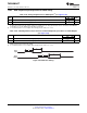


Table Of Contents
- 1 Digital Media System-on-Chip (DMSoC)
- Table of Contents
- 2 Revision History
- 3 Device Overview
- 3.1 Device Characteristics
- 3.2 Device Compatibility
- 3.3 ARM Subsystem
- 3.3.1 ARM926EJ-S RISC CPU
- 3.3.2 CP15
- 3.3.3 MMU
- 3.3.4 Caches and Write Buffer
- 3.3.5 Tightly Coupled Memory (TCM)
- 3.3.6 Advanced High-Performance Bus (AHB)
- 3.3.7 Embedded Trace Macrocell (ETM) and Embedded Trace Buffer (ETB)
- 3.3.8 ARM Memory Mapping
- 3.3.9 Peripherals
- 3.3.10 PLL Controller (PLLC)
- 3.3.11 Power and Sleep Controller (PSC)
- 3.3.12 ARM Interrupt Controller (AINTC)
- 3.3.13 System Module
- 3.3.14 Power Management
- 3.4 DSP Subsystem
- 3.5 Memory Map Summary
- 3.6 Pin Assignments
- 3.7 Terminal Functions
- 3.8 Device Support
- 3.9 Documentation Support
- 3.10 Community Resources
- 4 Device Configurations
- 4.1 System Module Registers
- 4.2 Power Considerations
- 4.3 Clock Considerations
- 4.4 Boot Sequence
- 4.5 Configurations At Reset
- 4.6 Configurations After Reset
- 4.7 Multiplexed Pin Configurations
- 4.7.1 Pin Muxing Selection At Reset
- 4.7.2 Pin Muxing Selection After Reset
- 4.7.3 Pin Multiplexing Details
- 4.7.3.1 PCI, HPI, EMIFA, and ATA Pin Muxing
- 4.7.3.2 PWM Signal Muxing
- 4.7.3.3 TSIF0 Input Signal Muxing (Serial/Parallel)
- 4.7.3.4 TSIF0 Output Signal Muxing (Serial/Parallel)
- 4.7.3.5 TSIF1 Input Signal Muxing (Serial Only)
- 4.7.3.6 TSIF1 Output Signal Muxing (Serial Only)
- 4.7.3.7 CRGEN Signal Muxing
- 4.7.3.8 UART0 Pin Muxing
- 4.7.3.9 UART1 Pin Muxing
- 4.7.3.10 UART2 Pin Muxing
- 4.7.3.11 ARM/DSP Communications Interrupts
- 4.7.3.12 Emulation Control
- 4.8 Debugging Considerations
- 5 System Interconnect
- 6 Device Operating Conditions
- 7 Peripheral Information and Electrical Specifications
- 7.1 Parameter Information
- 7.2 Recommended Clock and Control Signal Transition Behavior
- 7.3 Power Supplies
- 7.4 External Clock Input From DEV_MXI/DEV_CLKIN and AUX_MXI/AUX_CLKIN Pins
- 7.5 Clock PLLs
- 7.6 Enhanced Direct Memory Access (EDMA3) Controller
- 7.7 Reset
- 7.8 Interrupts
- 7.9 External Memory Interface (EMIF)
- 7.10 DDR2 Memory Controller
- 7.10.1 DDR2 Memory Controller Electrical Data/Timing
- 7.10.2 DDR2 Interface
- 7.10.2.1 DDR2 Interface Schematic
- 7.10.2.2 Compatible JEDEC DDR2 Devices
- 7.10.2.3 PCB Stackup
- 7.10.2.4 Placement
- 7.10.2.5 DDR2 Keep Out Region
- 7.10.2.6 Bulk Bypass Capacitors
- 7.10.2.7 High-Speed Bypass Capacitors
- 7.10.2.8 Net Classes
- 7.10.2.9 DDR2 Signal Termination
- 7.10.2.10 VREF Routing
- 7.10.2.11 DDR2 CK and ADDR_CTRL Routing
- 7.11 Video Port Interface (VPIF)
- 7.12 Transport Stream Interface (TSIF)
- 7.13 Clock Recovery Generator (CRGEN)
- 7.14 Video Data Conversion Engine (VDCE)
- 7.15 Peripheral Component Interconnect (PCI)
- 7.16 Ethernet MAC (EMAC)
- 7.17 Management Data Input/Output (MDIO)
- 7.18 Host-Port Interface (HPI) Peripheral
- 7.19 USB 2.0 [see Note]
- 7.20 ATA Controller
- 7.21 VLYNQ
- 7.22 Multichannel Audio Serial Port (McASP0/1) Peripherals
- 7.23 Serial Peripheral Interface (SPI)
- 7.24 Universal Asynchronouse Receiver/Transmitter (UART)
- 7.25 Inter-Integrated Circuit (I2C)
- 7.26 Pulse Width Modulator (PWM)
- 7.27 Timers
- 7.28 General-Purpose Input/Output (GPIO)
- 7.29 IEEE 1149.1 JTAG
- 8 Mechanical Packaging and Orderable Information
TMS320DM6467T
SPRS605C –JULY 2009–REVISED JUNE 2012
www.ti.com
Table 7-148. JTAG ID Register Selection Bit Descriptions
BIT NAME DESCRIPTION
31:28 VARIANT Variant (4-Bit) value. DM6467T value: 0001 [Silicon Revision 3.0 and later].
27:12 PART NUMBER Part Number (16-Bit) value. DM6467T value: 1011 0111 0111 0000.
11-1 MANUFACTURER Manufacturer (11-Bit) value. DM6467T value: 0000 0010 111.
0 LSB LSB. This bit is read as a "1" for DM6467T.
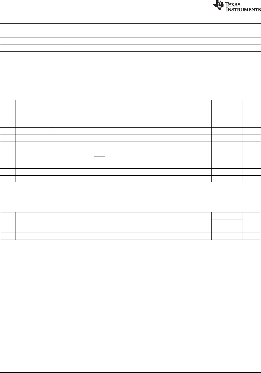
7.29.2 JTAG Test-Port Electrical Data/Timing
Table 7-149. Timing Requirements for JTAG Test Port
(1) (2)
(see Figure 7-96)
-1G
NO. UNIT
MIN MAX
1 t
c(TCK)
Cycle time, TCK 20 ns
2 t
w(TCKH)
Pulse duration, TCK high 0.4T ns
3 t
w(TCKL)
Pulse duration, TCK low 0.4T ns
4 t
c(RTCK)
Cycle time, RTCK 20 ns
5 t
w(RTCKH)
Pulse duration, RTCK high 0.4R ns
6 t
w(RTCKL)
Pulse duration, RTCK low 0.4R ns
7 t
su(TDIV-RTCKH)
Setup time, TDI/TMS/TRST valid before RTCK high 12 ns
8 t
h(RTCKH-TDIV)
Hold time, TDI/TMS/TRST valid after RTCK high 0 ns
9 t
su(EMUV-TCKH)
Setup time, EMU[1:0] valid before TCK high 1.5 ns
10 t
h(TCKH-EMUV)
Hold time, EMU[1:0] valid after TCK high 4 ns
(1) T = TCK cycle time in ns. For example, when TCK frequency is 20 MHz, use T = 50 ns.
(2) R = RTCLK cycle time in ns. For example, when RTCK frequency is 20 MHz, use T = 50 ns.
Table 7-150. Switching Characteristics Over Recommended Operating Conditions for JTAG Test Port
(1)
(see Figure 7-96)
-1G
NO. PARAMETER UNIT
MIN MAX
11 t
d(RTCKL-TDOV)
Delay time, RTCK low to TDO valid -1 8 ns
12 t
d(TCKH-EMUV)
Delay time, TCK high to EMU[1:0] valid 2.5 T - 2.5 ns
(1) T = TCK cycle time in ns. For example, when TCK frequency is 20 MHz, use T = 50 ns.
346 Peripheral Information and Electrical Specifications Copyright © 2009–2012, Texas Instruments Incorporated
Submit Documentation Feedback
Product Folder Link(s): TMS320DM6467T