
Datasheet


Table Of Contents
- 1 Digital Media System-on-Chip (DMSoC)
- Table of Contents
- 2 Revision History
- 3 Device Overview
- 3.1 Device Characteristics
- 3.2 Device Compatibility
- 3.3 ARM Subsystem
- 3.3.1 ARM926EJ-S RISC CPU
- 3.3.2 CP15
- 3.3.3 MMU
- 3.3.4 Caches and Write Buffer
- 3.3.5 Tightly Coupled Memory (TCM)
- 3.3.6 Advanced High-Performance Bus (AHB)
- 3.3.7 Embedded Trace Macrocell (ETM) and Embedded Trace Buffer (ETB)
- 3.3.8 ARM Memory Mapping
- 3.3.9 Peripherals
- 3.3.10 PLL Controller (PLLC)
- 3.3.11 Power and Sleep Controller (PSC)
- 3.3.12 ARM Interrupt Controller (AINTC)
- 3.3.13 System Module
- 3.3.14 Power Management
- 3.4 DSP Subsystem
- 3.5 Memory Map Summary
- 3.6 Pin Assignments
- 3.7 Terminal Functions
- 3.8 Device Support
- 3.9 Documentation Support
- 3.10 Community Resources
- 4 Device Configurations
- 4.1 System Module Registers
- 4.2 Power Considerations
- 4.3 Clock Considerations
- 4.4 Boot Sequence
- 4.5 Configurations At Reset
- 4.6 Configurations After Reset
- 4.7 Multiplexed Pin Configurations
- 4.7.1 Pin Muxing Selection At Reset
- 4.7.2 Pin Muxing Selection After Reset
- 4.7.3 Pin Multiplexing Details
- 4.7.3.1 PCI, HPI, EMIFA, and ATA Pin Muxing
- 4.7.3.2 PWM Signal Muxing
- 4.7.3.3 TSIF0 Input Signal Muxing (Serial/Parallel)
- 4.7.3.4 TSIF0 Output Signal Muxing (Serial/Parallel)
- 4.7.3.5 TSIF1 Input Signal Muxing (Serial Only)
- 4.7.3.6 TSIF1 Output Signal Muxing (Serial Only)
- 4.7.3.7 CRGEN Signal Muxing
- 4.7.3.8 UART0 Pin Muxing
- 4.7.3.9 UART1 Pin Muxing
- 4.7.3.10 UART2 Pin Muxing
- 4.7.3.11 ARM/DSP Communications Interrupts
- 4.7.3.12 Emulation Control
- 4.8 Debugging Considerations
- 5 System Interconnect
- 6 Device Operating Conditions
- 7 Peripheral Information and Electrical Specifications
- 7.1 Parameter Information
- 7.2 Recommended Clock and Control Signal Transition Behavior
- 7.3 Power Supplies
- 7.4 External Clock Input From DEV_MXI/DEV_CLKIN and AUX_MXI/AUX_CLKIN Pins
- 7.5 Clock PLLs
- 7.6 Enhanced Direct Memory Access (EDMA3) Controller
- 7.7 Reset
- 7.8 Interrupts
- 7.9 External Memory Interface (EMIF)
- 7.10 DDR2 Memory Controller
- 7.10.1 DDR2 Memory Controller Electrical Data/Timing
- 7.10.2 DDR2 Interface
- 7.10.2.1 DDR2 Interface Schematic
- 7.10.2.2 Compatible JEDEC DDR2 Devices
- 7.10.2.3 PCB Stackup
- 7.10.2.4 Placement
- 7.10.2.5 DDR2 Keep Out Region
- 7.10.2.6 Bulk Bypass Capacitors
- 7.10.2.7 High-Speed Bypass Capacitors
- 7.10.2.8 Net Classes
- 7.10.2.9 DDR2 Signal Termination
- 7.10.2.10 VREF Routing
- 7.10.2.11 DDR2 CK and ADDR_CTRL Routing
- 7.11 Video Port Interface (VPIF)
- 7.12 Transport Stream Interface (TSIF)
- 7.13 Clock Recovery Generator (CRGEN)
- 7.14 Video Data Conversion Engine (VDCE)
- 7.15 Peripheral Component Interconnect (PCI)
- 7.16 Ethernet MAC (EMAC)
- 7.17 Management Data Input/Output (MDIO)
- 7.18 Host-Port Interface (HPI) Peripheral
- 7.19 USB 2.0 [see Note]
- 7.20 ATA Controller
- 7.21 VLYNQ
- 7.22 Multichannel Audio Serial Port (McASP0/1) Peripherals
- 7.23 Serial Peripheral Interface (SPI)
- 7.24 Universal Asynchronouse Receiver/Transmitter (UART)
- 7.25 Inter-Integrated Circuit (I2C)
- 7.26 Pulse Width Modulator (PWM)
- 7.27 Timers
- 7.28 General-Purpose Input/Output (GPIO)
- 7.29 IEEE 1149.1 JTAG
- 8 Mechanical Packaging and Orderable Information
TMS320DM6467T
www.ti.com
SPRS605C –JULY 2009–REVISED JUNE 2012
7.29 IEEE 1149.1 JTAG
The JTAG
(3)
interface is used for BSDL testing and emulation of the DM6467T device.
TRST only needs to be released when it is necessary to use a JTAG controller to debug the device or
exercise the device's boundary scan functionality.
RESET must be released only in order for boundary-scan JTAG to read the variant field of IDCODE
correctly. Other boundary-scan instructions work correctly independent of current state of RESET.
DM6467T includes an internal pulldown (IPD) on the TRST pin to ensure that TRST will always be
asserted upon power up and the device's internal emulation logic will always be properly initialized.
JTAG controllers from Texas Instruments actively drive TRST high. However, some third-party JTAG
controllers may not drive TRST high but expect the use of a pullup resistor on TRST. When using this type
of JTAG controller, assert TRST to initialize the device after powerup and externally drive TRST high
before attempting any emulation or boundary scan operations.
7.29.1 JTAG ID (JTAGID) Register Description(s)
Table 7-147. JTAG ID Register
HEX ADDRESS RANGE ACRONYM REGISTER NAME COMMENTS
Read-only. Provides 32-bit
0x01C4 0028 JTAGID JTAG Identification Register
JTAG ID of the device.
(3) IEEE Standard 1149.1-1990 Standard-Test-Access Port and Boundary Scan Architecture.
The JTAG ID register is a read-only register that identifies to the customer the JTAG/Device ID. For the
DM6467T device, the JTAG ID register resides at address location 0x01C4 0028. The register hex value
for DM6467T is: 0x1B77 002F. For the actual register bit names and their associated bit field descriptions,
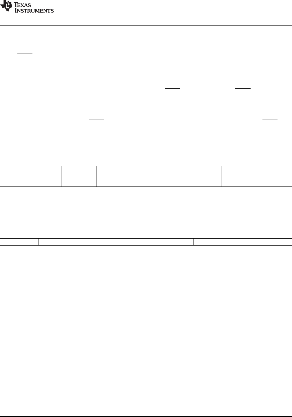
see Figure 7-95 and Table 7-148.
31-28 27-12 11-1 0
VARIANT (4-Bit) PART NUMBER (16-Bit) MANUFACTURER (11-Bit) LSB
R-0001 R-1011 0111 0111 0000 R-0000 0010 111 R-1
LEGEND: R = Read, W = Write, n = value at reset
Figure 7-95. JTAG ID Register Description - DM6467T Register Value - 0x1B77 002F
Copyright © 2009–2012, Texas Instruments Incorporated Peripheral Information and Electrical Specifications 345
Submit Documentation Feedback
Product Folder Link(s): TMS320DM6467T