
Datasheet


Table Of Contents
- 1 Digital Media System-on-Chip (DMSoC)
- Table of Contents
- 2 Revision History
- 3 Device Overview
- 3.1 Device Characteristics
- 3.2 Device Compatibility
- 3.3 ARM Subsystem
- 3.3.1 ARM926EJ-S RISC CPU
- 3.3.2 CP15
- 3.3.3 MMU
- 3.3.4 Caches and Write Buffer
- 3.3.5 Tightly Coupled Memory (TCM)
- 3.3.6 Advanced High-Performance Bus (AHB)
- 3.3.7 Embedded Trace Macrocell (ETM) and Embedded Trace Buffer (ETB)
- 3.3.8 ARM Memory Mapping
- 3.3.9 Peripherals
- 3.3.10 PLL Controller (PLLC)
- 3.3.11 Power and Sleep Controller (PSC)
- 3.3.12 ARM Interrupt Controller (AINTC)
- 3.3.13 System Module
- 3.3.14 Power Management
- 3.4 DSP Subsystem
- 3.5 Memory Map Summary
- 3.6 Pin Assignments
- 3.7 Terminal Functions
- 3.8 Device Support
- 3.9 Documentation Support
- 3.10 Community Resources
- 4 Device Configurations
- 4.1 System Module Registers
- 4.2 Power Considerations
- 4.3 Clock Considerations
- 4.4 Boot Sequence
- 4.5 Configurations At Reset
- 4.6 Configurations After Reset
- 4.7 Multiplexed Pin Configurations
- 4.7.1 Pin Muxing Selection At Reset
- 4.7.2 Pin Muxing Selection After Reset
- 4.7.3 Pin Multiplexing Details
- 4.7.3.1 PCI, HPI, EMIFA, and ATA Pin Muxing
- 4.7.3.2 PWM Signal Muxing
- 4.7.3.3 TSIF0 Input Signal Muxing (Serial/Parallel)
- 4.7.3.4 TSIF0 Output Signal Muxing (Serial/Parallel)
- 4.7.3.5 TSIF1 Input Signal Muxing (Serial Only)
- 4.7.3.6 TSIF1 Output Signal Muxing (Serial Only)
- 4.7.3.7 CRGEN Signal Muxing
- 4.7.3.8 UART0 Pin Muxing
- 4.7.3.9 UART1 Pin Muxing
- 4.7.3.10 UART2 Pin Muxing
- 4.7.3.11 ARM/DSP Communications Interrupts
- 4.7.3.12 Emulation Control
- 4.8 Debugging Considerations
- 5 System Interconnect
- 6 Device Operating Conditions
- 7 Peripheral Information and Electrical Specifications
- 7.1 Parameter Information
- 7.2 Recommended Clock and Control Signal Transition Behavior
- 7.3 Power Supplies
- 7.4 External Clock Input From DEV_MXI/DEV_CLKIN and AUX_MXI/AUX_CLKIN Pins
- 7.5 Clock PLLs
- 7.6 Enhanced Direct Memory Access (EDMA3) Controller
- 7.7 Reset
- 7.8 Interrupts
- 7.9 External Memory Interface (EMIF)
- 7.10 DDR2 Memory Controller
- 7.10.1 DDR2 Memory Controller Electrical Data/Timing
- 7.10.2 DDR2 Interface
- 7.10.2.1 DDR2 Interface Schematic
- 7.10.2.2 Compatible JEDEC DDR2 Devices
- 7.10.2.3 PCB Stackup
- 7.10.2.4 Placement
- 7.10.2.5 DDR2 Keep Out Region
- 7.10.2.6 Bulk Bypass Capacitors
- 7.10.2.7 High-Speed Bypass Capacitors
- 7.10.2.8 Net Classes
- 7.10.2.9 DDR2 Signal Termination
- 7.10.2.10 VREF Routing
- 7.10.2.11 DDR2 CK and ADDR_CTRL Routing
- 7.11 Video Port Interface (VPIF)
- 7.12 Transport Stream Interface (TSIF)
- 7.13 Clock Recovery Generator (CRGEN)
- 7.14 Video Data Conversion Engine (VDCE)
- 7.15 Peripheral Component Interconnect (PCI)
- 7.16 Ethernet MAC (EMAC)
- 7.17 Management Data Input/Output (MDIO)
- 7.18 Host-Port Interface (HPI) Peripheral
- 7.19 USB 2.0 [see Note]
- 7.20 ATA Controller
- 7.21 VLYNQ
- 7.22 Multichannel Audio Serial Port (McASP0/1) Peripherals
- 7.23 Serial Peripheral Interface (SPI)
- 7.24 Universal Asynchronouse Receiver/Transmitter (UART)
- 7.25 Inter-Integrated Circuit (I2C)
- 7.26 Pulse Width Modulator (PWM)
- 7.27 Timers
- 7.28 General-Purpose Input/Output (GPIO)
- 7.29 IEEE 1149.1 JTAG
- 8 Mechanical Packaging and Orderable Information
TMS320DM6467T
www.ti.com
SPRS605C –JULY 2009–REVISED JUNE 2012
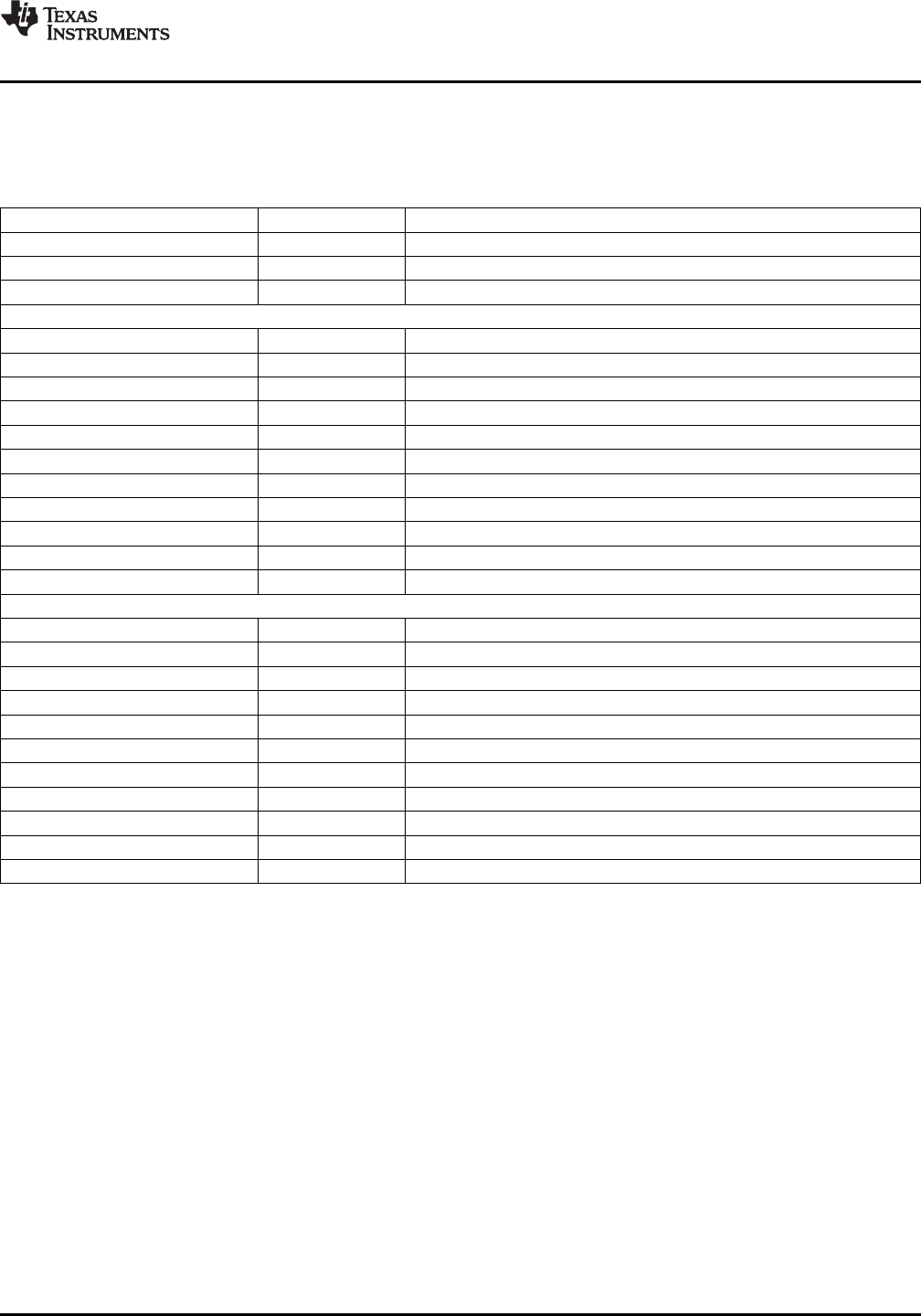
7.28.2 GPIO Peripheral Register Description(s)
Table 7-144 shows the GPIO peripheral registers.
Table 7-144. GPIO Registers
HEX ADDRESS RANGE ACRONYM REGISTER NAME
0x01C6 7000 PID Peripheral Identification Register
0x01C6 7004 - Reserved
0x01C6 7008 BINTEN GPIO interrupt per-bank enable
GPIO Banks 0 and 1
0x01C6 700C - Reserved
0x01C6 7010 DIR01 GPIO Banks 0 and 1 Direction Register (GP[0:31])
0x01C6 7014 OUT_DATA01 GPIO Banks 0 and 1 Output Data Register (GP[0:31])
0x01C6 7018 SET_DATA01 GPIO Banks 0 and 1 Set Data Register (GP[0:31])
0x01C6 701C CLR_DATA01 GPIO Banks 0 and 1 Clear data for banks 0 and 1 (GP[0:31])
0x01C6 7020 IN_DATA01 GPIO Banks 0 and 1 Input Data Register (GP[0:31])
0x01C6 7024 SET_RIS_TRIG01 GPIO Banks 0 and 1 Set Rising Edge Interrupt Register (GP[0:31])
0x01C6 7028 CLR_RIS_TRIG01 GPIO Banks 0 and 1 Clear Rising Edge Interrupt Register (GP[0:31])
0x01C6 702C SET_FAL_TRIG01 GPIO Banks 0 and 1 Set Falling Edge Interrupt Register (GP[0:31])
0x01C6 7030 CLR_FAL_TRIG01 GPIO Banks 0 and 1 Clear Falling Edge Interrupt Register (GP[0:31])
0x01C6 7034 INSTAT01 GPIO Banks 0 and 1 Interrupt Status Register (GP[0:31])
GPIO Bank 2
0x01C6 7038 DIR2 GPIO Bank 2 Direction Register (GP[32:47])
0x01C6 703C OUT_DATA2 GPIO Bank 2 Output Data Register (GP[32:47])
0x01C6 7040 SET_DATA2 GPIO Bank 2 Set Data Register (GP[32:47])
0x01C6 7044 CLR_DATA2 GPIO Bank 2 Clear Data Register (GP[32:47])
0x01C6 7048 IN_DATA2 GPIO Bank 2 Input Data Register (GP[32:47])
0x01C6 704C SET_RIS_TRIG2 GPIO Bank 2 Set Rising Edge Interrupt Register (GP[32:47])
0x01C6 7050 CLR_RIS_TRIG2 GPIO Bank 2 Clear Rising Edge Interrupt Register (GP[32:47])
0x01C6 7054 SET_FAL_TRIG2 GPIO Bank 2 Set Falling Edge Interrupt Register (GP[32:47])
0x01C6 7058 CLR_FAL_TRIG2 GPIO Bank 2 Clear Falling Edge Interrupt Register (GP[32:47])
0x01C6 705C INSTAT2 GPIO Bank 2 Interrupt Status Register (GP[32:47])
0x01C6 7060 - 0x01C6 77FF - Reserved
Copyright © 2009–2012, Texas Instruments Incorporated Peripheral Information and Electrical Specifications 343
Submit Documentation Feedback
Product Folder Link(s): TMS320DM6467T