
Datasheet


Table Of Contents
- 1 Digital Media System-on-Chip (DMSoC)
- Table of Contents
- 2 Revision History
- 3 Device Overview
- 3.1 Device Characteristics
- 3.2 Device Compatibility
- 3.3 ARM Subsystem
- 3.3.1 ARM926EJ-S RISC CPU
- 3.3.2 CP15
- 3.3.3 MMU
- 3.3.4 Caches and Write Buffer
- 3.3.5 Tightly Coupled Memory (TCM)
- 3.3.6 Advanced High-Performance Bus (AHB)
- 3.3.7 Embedded Trace Macrocell (ETM) and Embedded Trace Buffer (ETB)
- 3.3.8 ARM Memory Mapping
- 3.3.9 Peripherals
- 3.3.10 PLL Controller (PLLC)
- 3.3.11 Power and Sleep Controller (PSC)
- 3.3.12 ARM Interrupt Controller (AINTC)
- 3.3.13 System Module
- 3.3.14 Power Management
- 3.4 DSP Subsystem
- 3.5 Memory Map Summary
- 3.6 Pin Assignments
- 3.7 Terminal Functions
- 3.8 Device Support
- 3.9 Documentation Support
- 3.10 Community Resources
- 4 Device Configurations
- 4.1 System Module Registers
- 4.2 Power Considerations
- 4.3 Clock Considerations
- 4.4 Boot Sequence
- 4.5 Configurations At Reset
- 4.6 Configurations After Reset
- 4.7 Multiplexed Pin Configurations
- 4.7.1 Pin Muxing Selection At Reset
- 4.7.2 Pin Muxing Selection After Reset
- 4.7.3 Pin Multiplexing Details
- 4.7.3.1 PCI, HPI, EMIFA, and ATA Pin Muxing
- 4.7.3.2 PWM Signal Muxing
- 4.7.3.3 TSIF0 Input Signal Muxing (Serial/Parallel)
- 4.7.3.4 TSIF0 Output Signal Muxing (Serial/Parallel)
- 4.7.3.5 TSIF1 Input Signal Muxing (Serial Only)
- 4.7.3.6 TSIF1 Output Signal Muxing (Serial Only)
- 4.7.3.7 CRGEN Signal Muxing
- 4.7.3.8 UART0 Pin Muxing
- 4.7.3.9 UART1 Pin Muxing
- 4.7.3.10 UART2 Pin Muxing
- 4.7.3.11 ARM/DSP Communications Interrupts
- 4.7.3.12 Emulation Control
- 4.8 Debugging Considerations
- 5 System Interconnect
- 6 Device Operating Conditions
- 7 Peripheral Information and Electrical Specifications
- 7.1 Parameter Information
- 7.2 Recommended Clock and Control Signal Transition Behavior
- 7.3 Power Supplies
- 7.4 External Clock Input From DEV_MXI/DEV_CLKIN and AUX_MXI/AUX_CLKIN Pins
- 7.5 Clock PLLs
- 7.6 Enhanced Direct Memory Access (EDMA3) Controller
- 7.7 Reset
- 7.8 Interrupts
- 7.9 External Memory Interface (EMIF)
- 7.10 DDR2 Memory Controller
- 7.10.1 DDR2 Memory Controller Electrical Data/Timing
- 7.10.2 DDR2 Interface
- 7.10.2.1 DDR2 Interface Schematic
- 7.10.2.2 Compatible JEDEC DDR2 Devices
- 7.10.2.3 PCB Stackup
- 7.10.2.4 Placement
- 7.10.2.5 DDR2 Keep Out Region
- 7.10.2.6 Bulk Bypass Capacitors
- 7.10.2.7 High-Speed Bypass Capacitors
- 7.10.2.8 Net Classes
- 7.10.2.9 DDR2 Signal Termination
- 7.10.2.10 VREF Routing
- 7.10.2.11 DDR2 CK and ADDR_CTRL Routing
- 7.11 Video Port Interface (VPIF)
- 7.12 Transport Stream Interface (TSIF)
- 7.13 Clock Recovery Generator (CRGEN)
- 7.14 Video Data Conversion Engine (VDCE)
- 7.15 Peripheral Component Interconnect (PCI)
- 7.16 Ethernet MAC (EMAC)
- 7.17 Management Data Input/Output (MDIO)
- 7.18 Host-Port Interface (HPI) Peripheral
- 7.19 USB 2.0 [see Note]
- 7.20 ATA Controller
- 7.21 VLYNQ
- 7.22 Multichannel Audio Serial Port (McASP0/1) Peripherals
- 7.23 Serial Peripheral Interface (SPI)
- 7.24 Universal Asynchronouse Receiver/Transmitter (UART)
- 7.25 Inter-Integrated Circuit (I2C)
- 7.26 Pulse Width Modulator (PWM)
- 7.27 Timers
- 7.28 General-Purpose Input/Output (GPIO)
- 7.29 IEEE 1149.1 JTAG
- 8 Mechanical Packaging and Orderable Information
TMS320DM6467T
SPRS605C –JULY 2009–REVISED JUNE 2012
www.ti.com
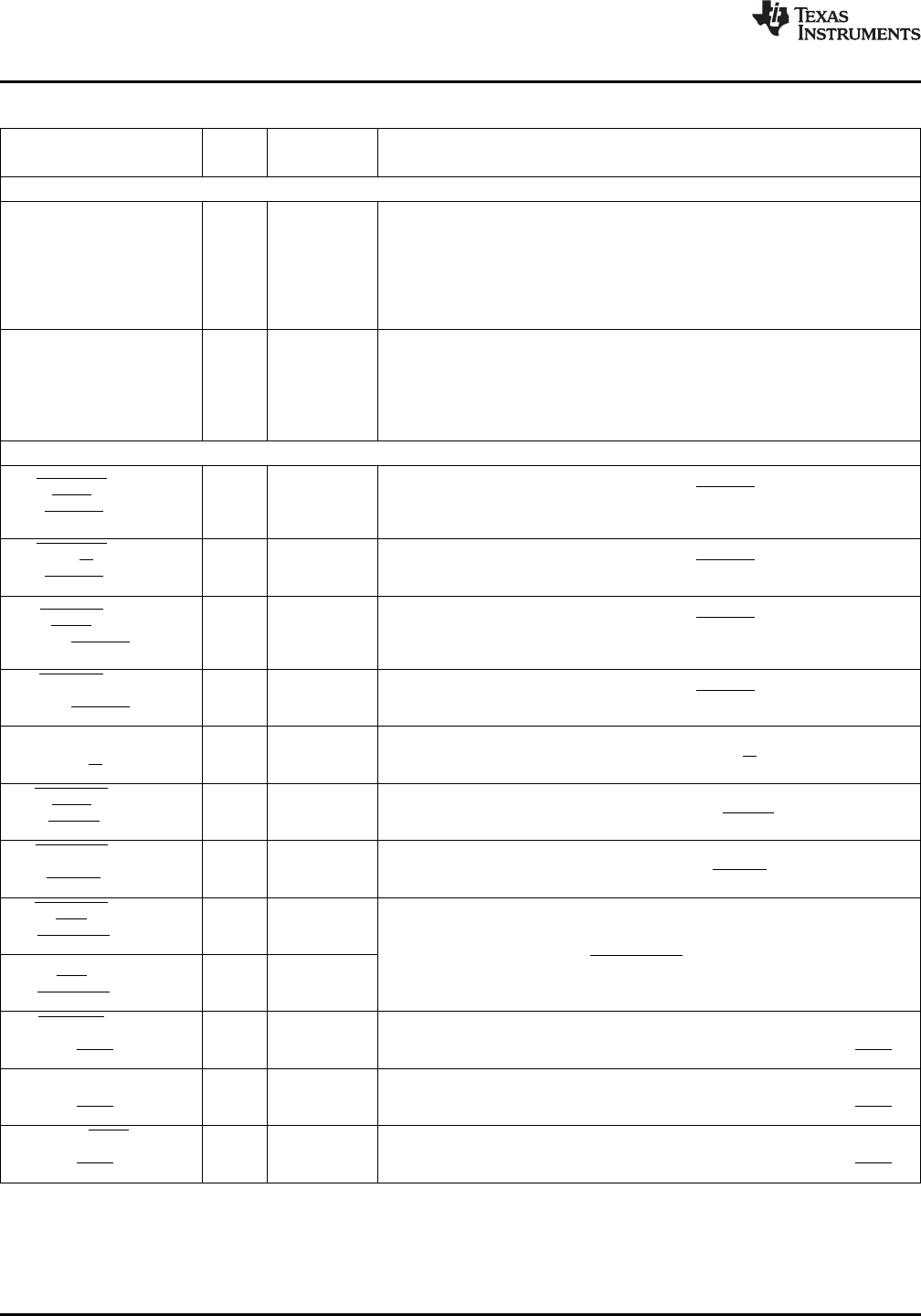
Table 3-9. Asynchronous External Memory Interface (EMIFA) Terminal Functions
SIGNAL
TYPE
(1)
OTHER
(2) (3)
DESCRIPTION
NAME NO.
EMIFA BOOT CONFIGURATION
EMIFA CS2 space data bus width. This pin is multiplexed between EMIFA control
and the VPIF. At reset, the input state is sampled to set the EMIFA data bus
width for the CS2 (boot) chip select region.
VP_DOUT4/ IPD
AA7 I/O/Z
CS2BW DV
DD33
For an 8-bit-wide EMIFA data bus, CS2BW = 0.
For a 16-bit-wide EMIFA data bus, CS2BW = 1.
After reset, this pin is video port data output 4 (VP_DOUT4).
DSP boot source bit. This pin is multiplexed between DSP boot and the VPIF. At
reset, the input state is sampled to set the DSP boot source DSPBOOT.
VP_DOUT6/ IPD
AC5 I/O/Z The DSP is booted by the ARM when DSPBOOT = 0.
DSPBOOT DV
DD33
The DSP boots from EMIFA when DSPBOOT=1.
After reset, this pin is video port data output 6 (VP_DOUT6).
EMIFA FUNCTIONAL PINS: ASYNC
This pin is multiplexed between PCI, HPI, and EMIFA.
PCI_CBE2/
IPU In EMIFA mode, this pin is Chip Select 2 output EM_CS2 (O/Z). This is the chip
HDS2/ C4 I/O/Z
DV
DD33
select used for EMIFA boot modes. Asynchronous memories (i.e., NOR Flash) or
EM_CS2
NAND flash.
PCI_CBE3/ This pin is multiplexed between PCI, HPI, and EMIFA.
IPU
HR/W A5 I/O/Z In EMIFA mode, this pin is Chip Select 3 output EM_CS3 (O/Z). Asynchronous
DV
DD33
EM_CS3 memories (i.e., NOR Flash).
This pin is multiplexed between PCI, ATA, GPIO, and EMIFA.
PCI_GNT/
IPU In EMIFA mode, this pin is Chip Select 4 output EM_CS4 (O/Z). Asynchronous
DACK/ D10 I/O/Z
DV
DD33
memories (i.e., NOR Flash).
GP[12]/ EM_CS4
This signal is not available when ATA is enabled (i.e., EMIF NAND Flash mode).
PCI_REQ/ This pin is multiplexed between PCI, ATA, GPIO, and EMIFA.
IPU
DMARQ/ B9 I/O/Z In EMIFA mode, this pin is Chip Select 5 output EM_CS5 (O/Z).
DV
DD33
GP[11]/ EM_CS5 This signal is not available when ATA is enabled (i.e., EMIF NAND Flash mode).
PCI_IDSEL/
IPU This pin is multiplexed between PCI, ATA, and EMIFA.
HDDIR/ E8 I/O/Z
DV
DD33
In EMIFA mode, this pin is the read/write output EM_R/W (O/Z).
EM_R/W
PCI_SERR/
IPU This pin is multiplexed between PCI, HPI, and EMIFA.
HDS1/ B2 I/O/Z
DV
DD33
In EMIFA mode, this pin is the output enable output EM_OE (O/Z).
EM_OE
PCI_STOP/
IPU This pin is multiplexed between PCI, HPI, and EMIFA.
HCNTL0/ D5 I/O/Z
DV
DD33
In EMIFA mode, this pin is the write enable output EM_WE (O/Z).
EM_WE
PCI_PERR/
IPU
HCS/ C3 I/O/Z
DV
DD33
EM_DQM1
These pins are multiplexed between PCI, HPI, and EMIFA.
In EMIFA mode, these pins are EM_DQM[1:0] and act as byte enables (O/Z).
PCI_PAR/
IPU
HAS/ D4 I/O/Z
DV
DD33
EM_DQM0
PCI_INTA/ This pin is multiplexed between PCI and EMIFA.
IPU
EM_WAIT2/ C11 I/O/Z In EMIFA mode, this pin is wait state extension input 2 EM_WAIT2 (I).
DV
DD33
(RDY2/BSY2) When used for EMIFA (NAND), this pin is the ready/busy 2 input (RDY2/BSY2).
PCI_RSV5/IORDY/ This pin is multiplexed between PCI, ATA, GPIO, and EMIFA.
IPU
GP[21]/EM_WAIT3/ D11 I/O/Z In EMIFA mode, this pin is wait state extension input 3 EM_WAIT3 (I).
DV
DD33
(RDY3/BSY3) When used for EMIFA (NAND), this pin is the ready/busy 3 input (RDY3/BSY3).
PCI_RSV4/DIOW/ This pin is multiplexed between PCI, ATA, GPIO, and EMIFA.
IPU
GP[20]/EM_WAIT4/ A11 I/O/Z In EMIFA mode, this pin is wait state extension input 4 EM_WAIT4 (I).
DV
DD33
(RDY4/BSY4) When used for EMIFA (NAND), this pin is the ready/busy 4 input (RDY4/BSY4).
(1) I = Input, O = Output, Z = High impedance, S = Supply voltage, GND = Ground, A = Analog signal
(2) IPD = Internal pulldown, IPU = Internal pullup. For more detailed information on pullup/pulldown resistors and situations where external
pullup/pulldown resistors are required, see Section 4.8.1, Pullup/Pulldown Resistors.
(3) Specifies the operating I/O supply voltage for each signal
34 Device Overview Copyright © 2009–2012, Texas Instruments Incorporated
Submit Documentation Feedback
Product Folder Link(s): TMS320DM6467T