
Datasheet


Table Of Contents
- 1 Digital Media System-on-Chip (DMSoC)
- Table of Contents
- 2 Revision History
- 3 Device Overview
- 3.1 Device Characteristics
- 3.2 Device Compatibility
- 3.3 ARM Subsystem
- 3.3.1 ARM926EJ-S RISC CPU
- 3.3.2 CP15
- 3.3.3 MMU
- 3.3.4 Caches and Write Buffer
- 3.3.5 Tightly Coupled Memory (TCM)
- 3.3.6 Advanced High-Performance Bus (AHB)
- 3.3.7 Embedded Trace Macrocell (ETM) and Embedded Trace Buffer (ETB)
- 3.3.8 ARM Memory Mapping
- 3.3.9 Peripherals
- 3.3.10 PLL Controller (PLLC)
- 3.3.11 Power and Sleep Controller (PSC)
- 3.3.12 ARM Interrupt Controller (AINTC)
- 3.3.13 System Module
- 3.3.14 Power Management
- 3.4 DSP Subsystem
- 3.5 Memory Map Summary
- 3.6 Pin Assignments
- 3.7 Terminal Functions
- 3.8 Device Support
- 3.9 Documentation Support
- 3.10 Community Resources
- 4 Device Configurations
- 4.1 System Module Registers
- 4.2 Power Considerations
- 4.3 Clock Considerations
- 4.4 Boot Sequence
- 4.5 Configurations At Reset
- 4.6 Configurations After Reset
- 4.7 Multiplexed Pin Configurations
- 4.7.1 Pin Muxing Selection At Reset
- 4.7.2 Pin Muxing Selection After Reset
- 4.7.3 Pin Multiplexing Details
- 4.7.3.1 PCI, HPI, EMIFA, and ATA Pin Muxing
- 4.7.3.2 PWM Signal Muxing
- 4.7.3.3 TSIF0 Input Signal Muxing (Serial/Parallel)
- 4.7.3.4 TSIF0 Output Signal Muxing (Serial/Parallel)
- 4.7.3.5 TSIF1 Input Signal Muxing (Serial Only)
- 4.7.3.6 TSIF1 Output Signal Muxing (Serial Only)
- 4.7.3.7 CRGEN Signal Muxing
- 4.7.3.8 UART0 Pin Muxing
- 4.7.3.9 UART1 Pin Muxing
- 4.7.3.10 UART2 Pin Muxing
- 4.7.3.11 ARM/DSP Communications Interrupts
- 4.7.3.12 Emulation Control
- 4.8 Debugging Considerations
- 5 System Interconnect
- 6 Device Operating Conditions
- 7 Peripheral Information and Electrical Specifications
- 7.1 Parameter Information
- 7.2 Recommended Clock and Control Signal Transition Behavior
- 7.3 Power Supplies
- 7.4 External Clock Input From DEV_MXI/DEV_CLKIN and AUX_MXI/AUX_CLKIN Pins
- 7.5 Clock PLLs
- 7.6 Enhanced Direct Memory Access (EDMA3) Controller
- 7.7 Reset
- 7.8 Interrupts
- 7.9 External Memory Interface (EMIF)
- 7.10 DDR2 Memory Controller
- 7.10.1 DDR2 Memory Controller Electrical Data/Timing
- 7.10.2 DDR2 Interface
- 7.10.2.1 DDR2 Interface Schematic
- 7.10.2.2 Compatible JEDEC DDR2 Devices
- 7.10.2.3 PCB Stackup
- 7.10.2.4 Placement
- 7.10.2.5 DDR2 Keep Out Region
- 7.10.2.6 Bulk Bypass Capacitors
- 7.10.2.7 High-Speed Bypass Capacitors
- 7.10.2.8 Net Classes
- 7.10.2.9 DDR2 Signal Termination
- 7.10.2.10 VREF Routing
- 7.10.2.11 DDR2 CK and ADDR_CTRL Routing
- 7.11 Video Port Interface (VPIF)
- 7.12 Transport Stream Interface (TSIF)
- 7.13 Clock Recovery Generator (CRGEN)
- 7.14 Video Data Conversion Engine (VDCE)
- 7.15 Peripheral Component Interconnect (PCI)
- 7.16 Ethernet MAC (EMAC)
- 7.17 Management Data Input/Output (MDIO)
- 7.18 Host-Port Interface (HPI) Peripheral
- 7.19 USB 2.0 [see Note]
- 7.20 ATA Controller
- 7.21 VLYNQ
- 7.22 Multichannel Audio Serial Port (McASP0/1) Peripherals
- 7.23 Serial Peripheral Interface (SPI)
- 7.24 Universal Asynchronouse Receiver/Transmitter (UART)
- 7.25 Inter-Integrated Circuit (I2C)
- 7.26 Pulse Width Modulator (PWM)
- 7.27 Timers
- 7.28 General-Purpose Input/Output (GPIO)
- 7.29 IEEE 1149.1 JTAG
- 8 Mechanical Packaging and Orderable Information
10
8
4
3
7
12
5
6
14
2
3
13
Stop Start Repeated
Start
Stop
SDA
SCL
1
11 9
TMS320DM6467T
www.ti.com
SPRS605C –JULY 2009–REVISED JUNE 2012
7.25.2 I2C Electrical Data/Timing
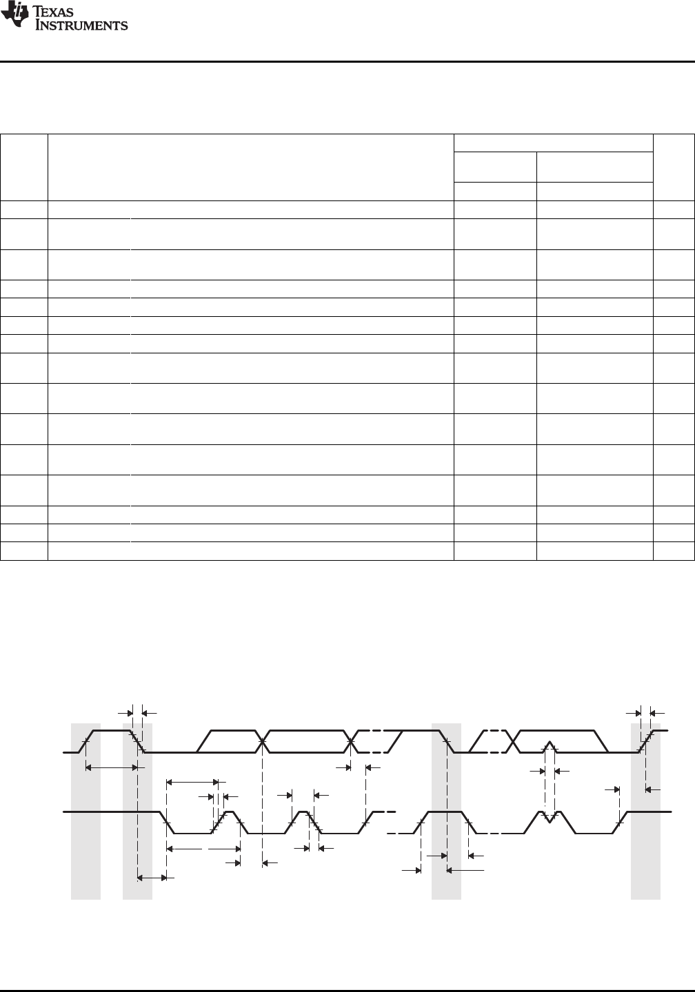
Table 7-134. Timing Requirements for I2C Timings
(1)
(see Figure 7-89)
-1G
STANDARD
NO. FAST MODE UNIT
MODE
MIN MAX MIN MAX
1 t
c(SCL)
Cycle time, SCL 10 2.5 µs
Setup time, SCL high before SDA low (for a repeated START
2 t
su(SCLH-SDAL)
4.7 0.6 µs
condition)
Hold time, SCL low after SDA low (for a START and a repeated
3 t
h(SCLL-SDAL)
4 0.6 µs
START condition)
4 t
w(SCLL)
Pulse duration, SCL low 4.7 1.3 µs
5 t
w(SCLH)
Pulse duration, SCL high 4 0.6 µs
6 t
su(SDAV-SCLH)
Setup time, SDA valid before SCL high 250 100
(2)
ns
7 t
h(SDA-SCLL)
Hold time, SDA valid after SCL low 0
(3)
0
(3)
0.9
(4)
µs
Pulse duration, SDA high between STOP and START
8 t
w(SDAH)
4.7 1.3 µs
conditions
20 + 0.1C
b
9 t
r(SDA)
Rise time, SDA 1000 300 ns
(5)
20 + 0.1C
b
10 t
r(SCL)
Rise time, SCL 1000 300 ns
(5)
20 + 0.1C
b
11 t
f(SDA)
Fall time, SDA 300 300 ns
(5)
20 + 0.1C
b
12 t
f(SCL)
Fall time, SCL 300 300 ns
(5)
13 t
su(SCLH-SDAH)
Setup time, SCL high before SDA high (for STOP condition) 4 0.6 µs
14 t
w(SP)
Pulse duration, spike (must be suppressed) 0 50 ns
15 C
b
(5)
Capacitive load for each bus line 400 400 pF
(1) The I2C pins SDA and SCL do not feature fail-safe I/O buffers. These pins could potentially draw current when the device is powered
down.
(2) A Fast-mode I
2
C-bus™ device can be used in a Standard-mode I
2
C-bus system, but the requirement t
su(SDA-SCLH)
≥ 250 ns must then be
met. This will automatically be the case if the device does not stretch the LOW period of the SCL signal. If such a device does stretch
the LOW period of the SCL signal, it must output the next data bit to the SDA line t
r
max + t
su(SDA-SCLH)
= 1000 + 250 = 1250 ns
(according to the Standard-mode I
2
C-Bus Specification) before the SCL line is released.
(3) A device must internally provide a hold time of at least 300 ns for the SDA signal (referred to the V
IHmin
of the SCL signal) to bridge the
undefined region of the falling edge of SCL.
(4) The maximum t
h(SDA-SCLL)
has only to be met if the device does not stretch the low period [t
w(SCLL)
] of the SCL signal.
(5) C
b
= total capacitance of one bus line in pF. If mixed with HS-mode devices, faster fall-times are allowed.
Figure 7-89. I2C Receive Timings
Copyright © 2009–2012, Texas Instruments Incorporated Peripheral Information and Electrical Specifications 335
Submit Documentation Feedback
Product Folder Link(s): TMS320DM6467T