
Datasheet


Table Of Contents
- 1 Digital Media System-on-Chip (DMSoC)
- Table of Contents
- 2 Revision History
- 3 Device Overview
- 3.1 Device Characteristics
- 3.2 Device Compatibility
- 3.3 ARM Subsystem
- 3.3.1 ARM926EJ-S RISC CPU
- 3.3.2 CP15
- 3.3.3 MMU
- 3.3.4 Caches and Write Buffer
- 3.3.5 Tightly Coupled Memory (TCM)
- 3.3.6 Advanced High-Performance Bus (AHB)
- 3.3.7 Embedded Trace Macrocell (ETM) and Embedded Trace Buffer (ETB)
- 3.3.8 ARM Memory Mapping
- 3.3.9 Peripherals
- 3.3.10 PLL Controller (PLLC)
- 3.3.11 Power and Sleep Controller (PSC)
- 3.3.12 ARM Interrupt Controller (AINTC)
- 3.3.13 System Module
- 3.3.14 Power Management
- 3.4 DSP Subsystem
- 3.5 Memory Map Summary
- 3.6 Pin Assignments
- 3.7 Terminal Functions
- 3.8 Device Support
- 3.9 Documentation Support
- 3.10 Community Resources
- 4 Device Configurations
- 4.1 System Module Registers
- 4.2 Power Considerations
- 4.3 Clock Considerations
- 4.4 Boot Sequence
- 4.5 Configurations At Reset
- 4.6 Configurations After Reset
- 4.7 Multiplexed Pin Configurations
- 4.7.1 Pin Muxing Selection At Reset
- 4.7.2 Pin Muxing Selection After Reset
- 4.7.3 Pin Multiplexing Details
- 4.7.3.1 PCI, HPI, EMIFA, and ATA Pin Muxing
- 4.7.3.2 PWM Signal Muxing
- 4.7.3.3 TSIF0 Input Signal Muxing (Serial/Parallel)
- 4.7.3.4 TSIF0 Output Signal Muxing (Serial/Parallel)
- 4.7.3.5 TSIF1 Input Signal Muxing (Serial Only)
- 4.7.3.6 TSIF1 Output Signal Muxing (Serial Only)
- 4.7.3.7 CRGEN Signal Muxing
- 4.7.3.8 UART0 Pin Muxing
- 4.7.3.9 UART1 Pin Muxing
- 4.7.3.10 UART2 Pin Muxing
- 4.7.3.11 ARM/DSP Communications Interrupts
- 4.7.3.12 Emulation Control
- 4.8 Debugging Considerations
- 5 System Interconnect
- 6 Device Operating Conditions
- 7 Peripheral Information and Electrical Specifications
- 7.1 Parameter Information
- 7.2 Recommended Clock and Control Signal Transition Behavior
- 7.3 Power Supplies
- 7.4 External Clock Input From DEV_MXI/DEV_CLKIN and AUX_MXI/AUX_CLKIN Pins
- 7.5 Clock PLLs
- 7.6 Enhanced Direct Memory Access (EDMA3) Controller
- 7.7 Reset
- 7.8 Interrupts
- 7.9 External Memory Interface (EMIF)
- 7.10 DDR2 Memory Controller
- 7.10.1 DDR2 Memory Controller Electrical Data/Timing
- 7.10.2 DDR2 Interface
- 7.10.2.1 DDR2 Interface Schematic
- 7.10.2.2 Compatible JEDEC DDR2 Devices
- 7.10.2.3 PCB Stackup
- 7.10.2.4 Placement
- 7.10.2.5 DDR2 Keep Out Region
- 7.10.2.6 Bulk Bypass Capacitors
- 7.10.2.7 High-Speed Bypass Capacitors
- 7.10.2.8 Net Classes
- 7.10.2.9 DDR2 Signal Termination
- 7.10.2.10 VREF Routing
- 7.10.2.11 DDR2 CK and ADDR_CTRL Routing
- 7.11 Video Port Interface (VPIF)
- 7.12 Transport Stream Interface (TSIF)
- 7.13 Clock Recovery Generator (CRGEN)
- 7.14 Video Data Conversion Engine (VDCE)
- 7.15 Peripheral Component Interconnect (PCI)
- 7.16 Ethernet MAC (EMAC)
- 7.17 Management Data Input/Output (MDIO)
- 7.18 Host-Port Interface (HPI) Peripheral
- 7.19 USB 2.0 [see Note]
- 7.20 ATA Controller
- 7.21 VLYNQ
- 7.22 Multichannel Audio Serial Port (McASP0/1) Peripherals
- 7.23 Serial Peripheral Interface (SPI)
- 7.24 Universal Asynchronouse Receiver/Transmitter (UART)
- 7.25 Inter-Integrated Circuit (I2C)
- 7.26 Pulse Width Modulator (PWM)
- 7.27 Timers
- 7.28 General-Purpose Input/Output (GPIO)
- 7.29 IEEE 1149.1 JTAG
- 8 Mechanical Packaging and Orderable Information
TMS320DM6467T
SPRS605C –JULY 2009–REVISED JUNE 2012
www.ti.com
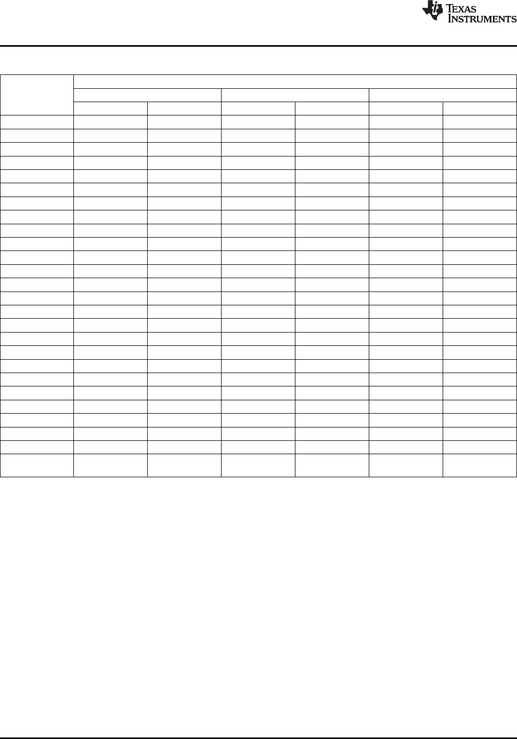
Table 7-127. UART2 – UART/IrDA/CIR Register Program Map
HEX ADDRESS REGISTER
RANGE
LCR[7] = 0 LCR[7] = 1 & LCR[7:0] ≠ 0xBF LCR[7:0] = 0xBF
READ WRITE READ WRITE READ WRITE
0x01C2 0800 RHR THR DLL DLL DLL DLL
0x01C2 0804 IER
(1)
IER
(1)
DLH DLH DLH DLH
0x01C2 0808 IIR FCR
(2)
IIR FCR
(2)
EFR EFR
0x01C2 080C LCR LCR LCR LCR LCR LCR
0x01C2 0810 MCR
(2)
MCR
(2)
MCR
(2)
MCR
(2)
XON1/ADDR1 XON1/ADDR1
0x01C2 0814 LSR – LSR – XON2/ADR2 XON2/ADDR2
0x01C2 0818 MSR/TCR
(3)
TCR
(3)
MSR/TCR
(3)
TCR
(3)
XOFF1/TCR
(3)
XOFF1/TCR
(3)
0x01C2 081C SPR/TLR
(3)
SPR/TLR
(3)
SPR/TLR
(3)
SPR/TLR
(3)
XOFF2/TLR
(3)
XOFF2/TLR
(3)
0x01C2 0820 MDR1 MDR1 MDR1 MDR1 MDR1 MDR1
0x01C2 0824 MDR2 MDR2 MDR2 MDR2 MDR2 MDR2
0x01C2 0828 SFLSR TXFLL SFLSR TXFLL SFLSR TXFLL
0x01C2 082C RESUME TXFLH RESUME TXFLH RESUME TXFLH
0x01C2 0830 SFREGL RXFLL SFREGL RXFLL SFREGL RXFLL
0x01C2 0834 SFREGH RXFLH SFREGH RXFLH SFREGH RXFLH
0x01C2 0838 BLR BLR UASR – UASR –
0x01C2 083C ACREG ACREG – – – –
0x01C2 0840 SCR SCR SCR SCR SCR SCR
0x01C2 0844 SSR – SSR – SSR –
0x01C2 0848 EBLR EBLR – – – –
0x01C2 084C – – – – – –
0x01C2 0850 MVR – MVR – MVR –
0x01C2 0854 SYSC SYSC SYSC SYSC SYSC SYSC
0x01C2 0858 SYSS – SYSS – SYSS –
0x01C2 085C WER WER WER WER WER WER
0x01C2 0860 CFPS CFPS CFPS CFPS CFPS CFPS
0x01C2 0864 - – – – – – –
0x01C2 087F
(1) In UART modes, IER.[7:4] can only be written when ENHANCED_EN in EFR = 1. In IrDA/CIR modes, ENHANCED_EN in EFR has no
impact on the access to IER.[7:4].
(2) MCR.[7:5] and the TX_FIFO_TRIG bits in FCR can only be written to when the ENHANCED_EN bit in EFR = 1.
(3) Transmission control register (TCR) and trigger level register (TLR) are accessible only when the ENHANCED_EN bit in the EFR =1
and the TCR_TLR bit in the MCR = 1.
330 Peripheral Information and Electrical Specifications Copyright © 2009–2012, Texas Instruments Incorporated
Submit Documentation Feedback
Product Folder Link(s): TMS320DM6467T