
Datasheet


Table Of Contents
- 1 Digital Media System-on-Chip (DMSoC)
- Table of Contents
- 2 Revision History
- 3 Device Overview
- 3.1 Device Characteristics
- 3.2 Device Compatibility
- 3.3 ARM Subsystem
- 3.3.1 ARM926EJ-S RISC CPU
- 3.3.2 CP15
- 3.3.3 MMU
- 3.3.4 Caches and Write Buffer
- 3.3.5 Tightly Coupled Memory (TCM)
- 3.3.6 Advanced High-Performance Bus (AHB)
- 3.3.7 Embedded Trace Macrocell (ETM) and Embedded Trace Buffer (ETB)
- 3.3.8 ARM Memory Mapping
- 3.3.9 Peripherals
- 3.3.10 PLL Controller (PLLC)
- 3.3.11 Power and Sleep Controller (PSC)
- 3.3.12 ARM Interrupt Controller (AINTC)
- 3.3.13 System Module
- 3.3.14 Power Management
- 3.4 DSP Subsystem
- 3.5 Memory Map Summary
- 3.6 Pin Assignments
- 3.7 Terminal Functions
- 3.8 Device Support
- 3.9 Documentation Support
- 3.10 Community Resources
- 4 Device Configurations
- 4.1 System Module Registers
- 4.2 Power Considerations
- 4.3 Clock Considerations
- 4.4 Boot Sequence
- 4.5 Configurations At Reset
- 4.6 Configurations After Reset
- 4.7 Multiplexed Pin Configurations
- 4.7.1 Pin Muxing Selection At Reset
- 4.7.2 Pin Muxing Selection After Reset
- 4.7.3 Pin Multiplexing Details
- 4.7.3.1 PCI, HPI, EMIFA, and ATA Pin Muxing
- 4.7.3.2 PWM Signal Muxing
- 4.7.3.3 TSIF0 Input Signal Muxing (Serial/Parallel)
- 4.7.3.4 TSIF0 Output Signal Muxing (Serial/Parallel)
- 4.7.3.5 TSIF1 Input Signal Muxing (Serial Only)
- 4.7.3.6 TSIF1 Output Signal Muxing (Serial Only)
- 4.7.3.7 CRGEN Signal Muxing
- 4.7.3.8 UART0 Pin Muxing
- 4.7.3.9 UART1 Pin Muxing
- 4.7.3.10 UART2 Pin Muxing
- 4.7.3.11 ARM/DSP Communications Interrupts
- 4.7.3.12 Emulation Control
- 4.8 Debugging Considerations
- 5 System Interconnect
- 6 Device Operating Conditions
- 7 Peripheral Information and Electrical Specifications
- 7.1 Parameter Information
- 7.2 Recommended Clock and Control Signal Transition Behavior
- 7.3 Power Supplies
- 7.4 External Clock Input From DEV_MXI/DEV_CLKIN and AUX_MXI/AUX_CLKIN Pins
- 7.5 Clock PLLs
- 7.6 Enhanced Direct Memory Access (EDMA3) Controller
- 7.7 Reset
- 7.8 Interrupts
- 7.9 External Memory Interface (EMIF)
- 7.10 DDR2 Memory Controller
- 7.10.1 DDR2 Memory Controller Electrical Data/Timing
- 7.10.2 DDR2 Interface
- 7.10.2.1 DDR2 Interface Schematic
- 7.10.2.2 Compatible JEDEC DDR2 Devices
- 7.10.2.3 PCB Stackup
- 7.10.2.4 Placement
- 7.10.2.5 DDR2 Keep Out Region
- 7.10.2.6 Bulk Bypass Capacitors
- 7.10.2.7 High-Speed Bypass Capacitors
- 7.10.2.8 Net Classes
- 7.10.2.9 DDR2 Signal Termination
- 7.10.2.10 VREF Routing
- 7.10.2.11 DDR2 CK and ADDR_CTRL Routing
- 7.11 Video Port Interface (VPIF)
- 7.12 Transport Stream Interface (TSIF)
- 7.13 Clock Recovery Generator (CRGEN)
- 7.14 Video Data Conversion Engine (VDCE)
- 7.15 Peripheral Component Interconnect (PCI)
- 7.16 Ethernet MAC (EMAC)
- 7.17 Management Data Input/Output (MDIO)
- 7.18 Host-Port Interface (HPI) Peripheral
- 7.19 USB 2.0 [see Note]
- 7.20 ATA Controller
- 7.21 VLYNQ
- 7.22 Multichannel Audio Serial Port (McASP0/1) Peripherals
- 7.23 Serial Peripheral Interface (SPI)
- 7.24 Universal Asynchronouse Receiver/Transmitter (UART)
- 7.25 Inter-Integrated Circuit (I2C)
- 7.26 Pulse Width Modulator (PWM)
- 7.27 Timers
- 7.28 General-Purpose Input/Output (GPIO)
- 7.29 IEEE 1149.1 JTAG
- 8 Mechanical Packaging and Orderable Information
TMS320DM6467T
SPRS605C –JULY 2009–REVISED JUNE 2012
www.ti.com
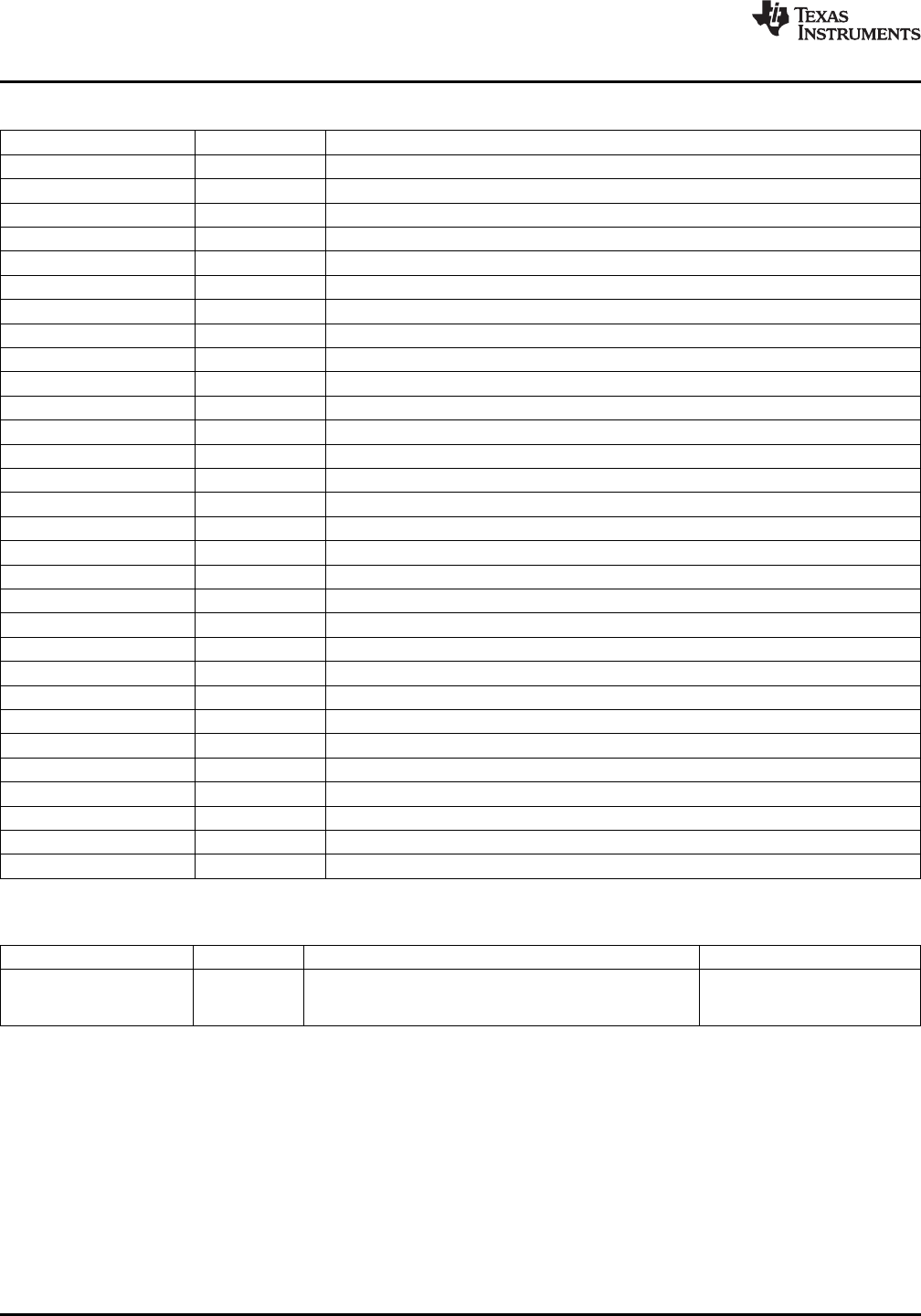
Table 7-103. McASP1 Control Registers (continued)
HEX ADDRESS RANGE ACRONYM REGISTER NAME
01D0 18D0 – 01D0 18FF – Reserved
01D0 1900 DITCSRA0 Left (even TDM slot) channel status register file
01D0 1904 DITCSRA1 Left (even TDM slot) channel status register file
01D0 1908 DITCSRA2 Left (even TDM slot) channel status register file
01D0 190C DITCSRA3 Left (even TDM slot) channel status register file
01D0 1910 DITCSRA4 Left (even TDM slot) channel status register file
01D0 1914 DITCSRA5 Left (even TDM slot) channel status register file
01D0 1918 DITCSRB0 Right (odd TDM slot) channel status register file
01D0 191C DITCSRB1 Right (odd TDM slot) channel status register file
01D0 1920 DITCSRB2 Right (odd TDM slot) channel status register file
01D0 1924 DITCSRB3 Right (odd TDM slot) channel status register file
01D0 1928 DITCSRB4 Right (odd TDM slot) channel status register file
01D0 192C DITCSRB5 Right (odd TDM slot) channel status register file
01D0 1930 DITUDRA0 Left (even TDM slot) user data register file
01D0 1934 DITUDRA1 Left (even TDM slot) user data register file
01D0 1938 DITUDRA2 Left (even TDM slot) user data register file
01D0 193C DITUDRA3 Left (even TDM slot) user data register file
01D0 1940 DITUDRA4 Left (even TDM slot) user data register file
01D0 1944 DITUDRA5 Left (even TDM slot) user data register file
01D0 1948 DITUDRB0 Right (odd TDM slot) user data register file
01D0 194C DITUDRB1 Right (odd TDM slot) user data register file
01D0 1950 DITUDRB2 Right (odd TDM slot) user data register file
01D0 1954 DITUDRB3 Right (odd TDM slot) user data register file
01D0 1958 DITUDRB4 Right (odd TDM slot) user data register file
01D0 195C DITUDRB5 Right (odd TDM slot) user data register file
01D0 1960 – 01D0 197F – Reserved
01D0 1980 SRCTL0 Serializer 0 control register
01D0 1984 – 01D0 19FF – Reserved
01D0 1A00 XBUF0 Transmit Buffer for Serializer 0
01D0 1A04 – 01D0 13FF – Reserved
Table 7-104. McASP1 Data Registers
HEX ADDRESS RANGE ACRONYM REGISTER NAME COMMENTS
(Used when XSEL bits = 0
01D0 1C00 – 01D0 1FFF XBUF1 McASP1 transmit buffers via the Peripheral Data Bus. [these bits are located in the
XFMT register].)
304 Peripheral Information and Electrical Specifications Copyright © 2009–2012, Texas Instruments Incorporated
Submit Documentation Feedback
Product Folder Link(s): TMS320DM6467T