
Datasheet


Table Of Contents
- 1 Digital Media System-on-Chip (DMSoC)
- Table of Contents
- 2 Revision History
- 3 Device Overview
- 3.1 Device Characteristics
- 3.2 Device Compatibility
- 3.3 ARM Subsystem
- 3.3.1 ARM926EJ-S RISC CPU
- 3.3.2 CP15
- 3.3.3 MMU
- 3.3.4 Caches and Write Buffer
- 3.3.5 Tightly Coupled Memory (TCM)
- 3.3.6 Advanced High-Performance Bus (AHB)
- 3.3.7 Embedded Trace Macrocell (ETM) and Embedded Trace Buffer (ETB)
- 3.3.8 ARM Memory Mapping
- 3.3.9 Peripherals
- 3.3.10 PLL Controller (PLLC)
- 3.3.11 Power and Sleep Controller (PSC)
- 3.3.12 ARM Interrupt Controller (AINTC)
- 3.3.13 System Module
- 3.3.14 Power Management
- 3.4 DSP Subsystem
- 3.5 Memory Map Summary
- 3.6 Pin Assignments
- 3.7 Terminal Functions
- 3.8 Device Support
- 3.9 Documentation Support
- 3.10 Community Resources
- 4 Device Configurations
- 4.1 System Module Registers
- 4.2 Power Considerations
- 4.3 Clock Considerations
- 4.4 Boot Sequence
- 4.5 Configurations At Reset
- 4.6 Configurations After Reset
- 4.7 Multiplexed Pin Configurations
- 4.7.1 Pin Muxing Selection At Reset
- 4.7.2 Pin Muxing Selection After Reset
- 4.7.3 Pin Multiplexing Details
- 4.7.3.1 PCI, HPI, EMIFA, and ATA Pin Muxing
- 4.7.3.2 PWM Signal Muxing
- 4.7.3.3 TSIF0 Input Signal Muxing (Serial/Parallel)
- 4.7.3.4 TSIF0 Output Signal Muxing (Serial/Parallel)
- 4.7.3.5 TSIF1 Input Signal Muxing (Serial Only)
- 4.7.3.6 TSIF1 Output Signal Muxing (Serial Only)
- 4.7.3.7 CRGEN Signal Muxing
- 4.7.3.8 UART0 Pin Muxing
- 4.7.3.9 UART1 Pin Muxing
- 4.7.3.10 UART2 Pin Muxing
- 4.7.3.11 ARM/DSP Communications Interrupts
- 4.7.3.12 Emulation Control
- 4.8 Debugging Considerations
- 5 System Interconnect
- 6 Device Operating Conditions
- 7 Peripheral Information and Electrical Specifications
- 7.1 Parameter Information
- 7.2 Recommended Clock and Control Signal Transition Behavior
- 7.3 Power Supplies
- 7.4 External Clock Input From DEV_MXI/DEV_CLKIN and AUX_MXI/AUX_CLKIN Pins
- 7.5 Clock PLLs
- 7.6 Enhanced Direct Memory Access (EDMA3) Controller
- 7.7 Reset
- 7.8 Interrupts
- 7.9 External Memory Interface (EMIF)
- 7.10 DDR2 Memory Controller
- 7.10.1 DDR2 Memory Controller Electrical Data/Timing
- 7.10.2 DDR2 Interface
- 7.10.2.1 DDR2 Interface Schematic
- 7.10.2.2 Compatible JEDEC DDR2 Devices
- 7.10.2.3 PCB Stackup
- 7.10.2.4 Placement
- 7.10.2.5 DDR2 Keep Out Region
- 7.10.2.6 Bulk Bypass Capacitors
- 7.10.2.7 High-Speed Bypass Capacitors
- 7.10.2.8 Net Classes
- 7.10.2.9 DDR2 Signal Termination
- 7.10.2.10 VREF Routing
- 7.10.2.11 DDR2 CK and ADDR_CTRL Routing
- 7.11 Video Port Interface (VPIF)
- 7.12 Transport Stream Interface (TSIF)
- 7.13 Clock Recovery Generator (CRGEN)
- 7.14 Video Data Conversion Engine (VDCE)
- 7.15 Peripheral Component Interconnect (PCI)
- 7.16 Ethernet MAC (EMAC)
- 7.17 Management Data Input/Output (MDIO)
- 7.18 Host-Port Interface (HPI) Peripheral
- 7.19 USB 2.0 [see Note]
- 7.20 ATA Controller
- 7.21 VLYNQ
- 7.22 Multichannel Audio Serial Port (McASP0/1) Peripherals
- 7.23 Serial Peripheral Interface (SPI)
- 7.24 Universal Asynchronouse Receiver/Transmitter (UART)
- 7.25 Inter-Integrated Circuit (I2C)
- 7.26 Pulse Width Modulator (PWM)
- 7.27 Timers
- 7.28 General-Purpose Input/Output (GPIO)
- 7.29 IEEE 1149.1 JTAG
- 8 Mechanical Packaging and Orderable Information
TMS320DM6467T
www.ti.com
SPRS605C –JULY 2009–REVISED JUNE 2012
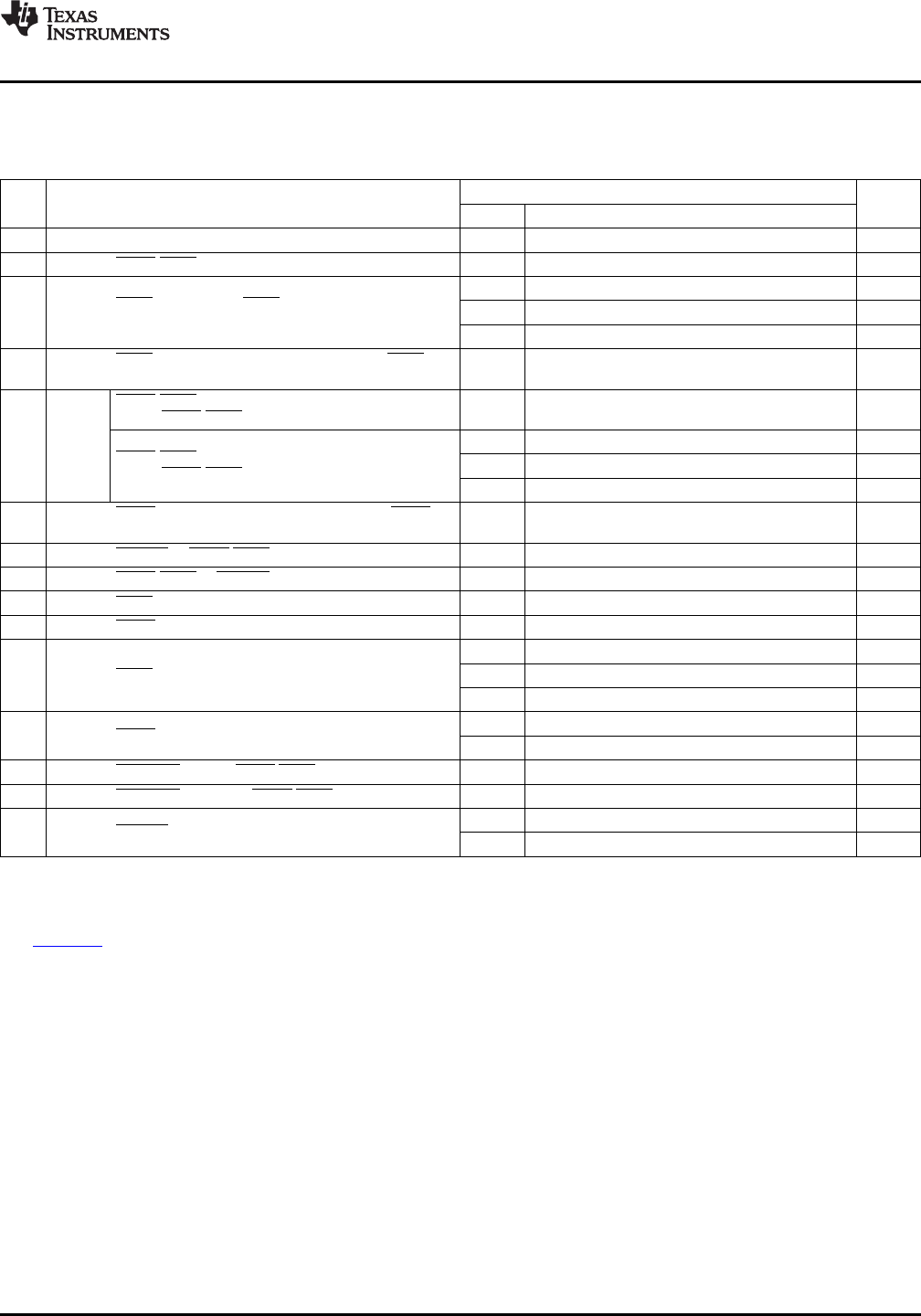
7.20.3.2 ATA Multiword DMA Timing
Table 7-91. Timings for ATA Module — Multiword DMA AC Timing
(1) (2)
(see Figure 7-65)
-1G
NO. UNIT
MODE MIN MAX
1 t
0
Cycle time 0-2 (DMASTB + DMARCVR + 2)P - 0.5 ns
2 t
D
DIOW/DIOR active low pulse duration 0-2 (DMASTB + 1)P - 1 ns
0 150 ns
DIOR data access, DIOR falling edge to DD[15:0]
3 t
E
1 60 ns
valid
2 50 ns
DIOR data hold time, DD[15:0] valid after DIOR
4 t
F
0-2 5 ns
rising edge
DIOW/DIOR data setup time, DD[15:0] (OUT) valid
0-2 (DMASTB)P ns
before DIOW/DIOR rising edge
0 100 ns
5 t
G
DIOW/DIOR data setup time, DD[15:0] (IN) valid
1 30 ns
before DIOW/DIOR rising edge
2 20 ns
DIOW data hold time, DD[15:0] valid after DIOW
6 t
H
0-2 (HWNHLD + 1)P + 1 ns
rising edge
7 t
I
DMACK to DIOW/DIOR setup 0-2 (DMARCVR + 1)P - 1.7 ns
8 t
J
DIOW/DIOR to DMACK hold 0-2 5P - 5.9 ns
9 t
KR
DIOR negated pulse width 0-2 (DMARCVR + 1)P - 1 ns
10 t
KW
DIOW negated pulse width 0-2 (DMARCVR + 1)P - 1 ns
0 120 ns
11 t
LR
DIOR to DMARQ delay 1 45 ns
2 35 ns
0-1 40 ns
12 t
LW
DIOW to DMARQ delay
2 35 ns
13 t
M
ATA_CSx valid to DIOW/DIOR setup 0-2 (DATRCVR)P - 1.7 ns
14 t
N
ATA_CSx valid after DIOW/DIOR rising edge hold 0-2 5P - 1.7 ns
0 20 ns
15 t
Z
DMACK to read data (DD[15:0]) released
1-2 25 ns
(1) P = SYSCLK4 period, in ns, for ATA. For example, when running the DSP CPU at 1 GHz, use P = 7 ns.
(2) DMASTB equals the value programmed in the DMASTBxP bit field in the DMASTB register. DMARCVR equals the value programmed
in the DMARCVRxP bit field in the DMARCVR register. HWNHLD equals the value programmed in the HWNHLDxP bit field in the
MISCCTL register. For more detailed information, see the TMS320DM646x DMSoC ATA Controller User's Guide (literature number
SPRUEQ3).
Copyright © 2009–2012, Texas Instruments Incorporated Peripheral Information and Electrical Specifications 283
Submit Documentation Feedback
Product Folder Link(s): TMS320DM6467T